A8740 Просмотр технического описания (PDF) - Allegro MicroSystems
Номер в каталоге
Компоненты Описание
Список матч
A8740
Allegro MicroSystems

A8740 Datasheet PDF : 18 Pages
| |||
A8740
Ultra Small Mobile Phone Xenon Photoflash
Capacitor Charger with IGBT Driver
Functional Description
General Operation Overview
The charging operation is started by a low-to-high signal on the
CHARGE pin, provided that VIN is above the VUVLO level. It is
strongly recommended to keep the CHARGE pin at logic low
during power-up. After VIN exceeds the UVLO level, a low-
to-high transition on the CHARGE pin is required to start the
charging. The ¯D¯¯¯O¯¯¯N¯¯E¯ open-drain indicator is pulled low when
CHARGE is high and target output voltage is reached.
When a charging cycle is initiated, the transformer primary side
current, IPRIMARY, ramps-up linearly at a rate determined by the
combined effect of the battery voltage, VBAT , and the primary
side inductance, LPRIMARY . When IPRIMARY reaches the current
limit, ISWLIM , the internal MOSFET is turned off immediately,
allowing the energy to be pushed into the photoflash capacitor,
COUT , from the secondary winding. The secondary side current
drops linearly as COUT charges. The switching cycle starts again,
either after the transformer flux is reset, or after a predetermined
time period, tOFF(max) (18 μs), whichever occurs first.
The A8740 senses output voltage indirectly on primary side. This
eliminates the need for high voltage feedback resistors required
for secondary sensing. Flyback converter stops switching when
output voltage reaches:
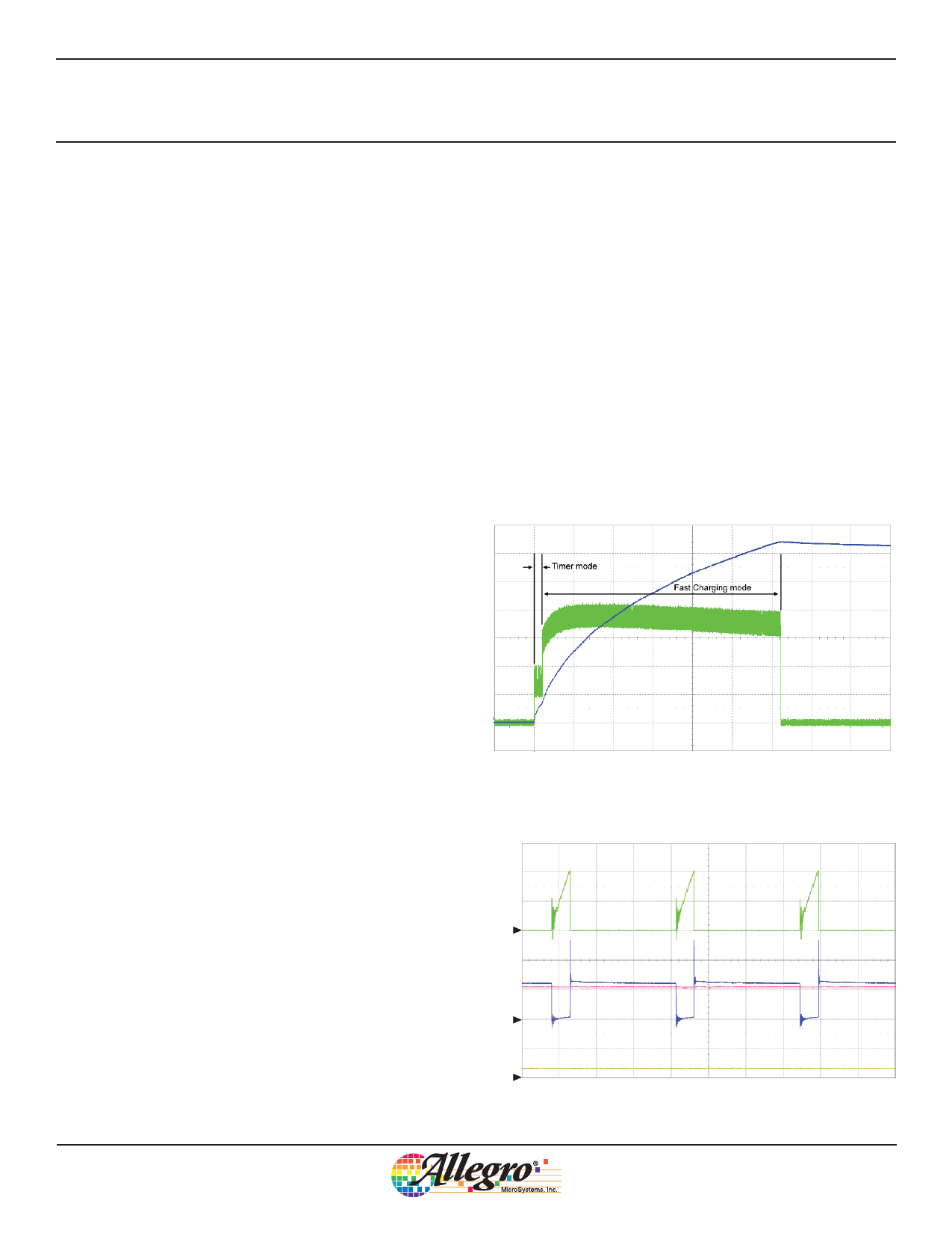
Timer Mode and Fast Charging Mode
The A8740 achieves fast charging times and high efficiency by
operating in discontinuous conduction mode (DCM) through
most of the charging process. The relationship of Timer mode and
Fast Charging mode is shown in figure 2.
The IC operates in Timer mode when beginning to charge a com-
pletely discharged photoflash capacitor, usually when the output
voltage, VOUT , is less than approximately 30 V (depending on
transformer used). Timer mode is a fixed period, 18 μs, off-time
control. One advantage of having Timer mode is that it limits the
initial battery current surge and thus acts as a “soft-start.” A time-
expanded view of a Timer mode interval is shown in figure 3.
VOUT
IIN
Where:
VOUT = K × N – Vd ,
K = 31.5 V typically,
Figure 2. Timer mode and Fast Charging mode: t = 1 s/div;
VOUT = 50 V/div; IIN = 150 mA/div., VIN = VBAT = 3.6 V;
COUT = 100 μF / 330 V; and ILIM = 1.0 A.
Vd is the forward drop of the output diode (approximately 2 V),
and
N is transformer turns ratio.
Switch On-Time and Off-Time Control
The A8740 implements an adaptive on-time/off-time control. On-
time duration, ton , is approximately equal to
ton = ISWlim × LPRIMARY / VBAT .
Off-time duration, toff , depends on the operating conditions
during switch off-time. The A8740 applies two charging modes:
Fast Charging mode and Timer mode, according to the conditions
described in the next section.
ISW
C4
C2,C3
VSW
VBAT
VOUT
C1
Figure 3. Expanded view of Timer mode: VOUT ≤ 10 V, VBAT = 5.5 V,
Ch1: VOUT = 20 V / div., Ch2: VBAT = 5 V / div., Ch3: VSW = 5 V / div.,
Ch4: ISW = 750 mA / div., t = 5 μs / div.
Allegro MicroSystems, Inc.
10
115 Northeast Cutoff
Worcester, Massachusetts 01615-0036 U.S.A.
1.508.853.5000; www.allegromicro.com
Share Link: