TJ20A10M3 Просмотр технического описания (PDF) - Toshiba
Номер в каталоге
Компоненты Описание
Список матч
TJ20A10M3 Datasheet PDF : 6 Pages
| |||
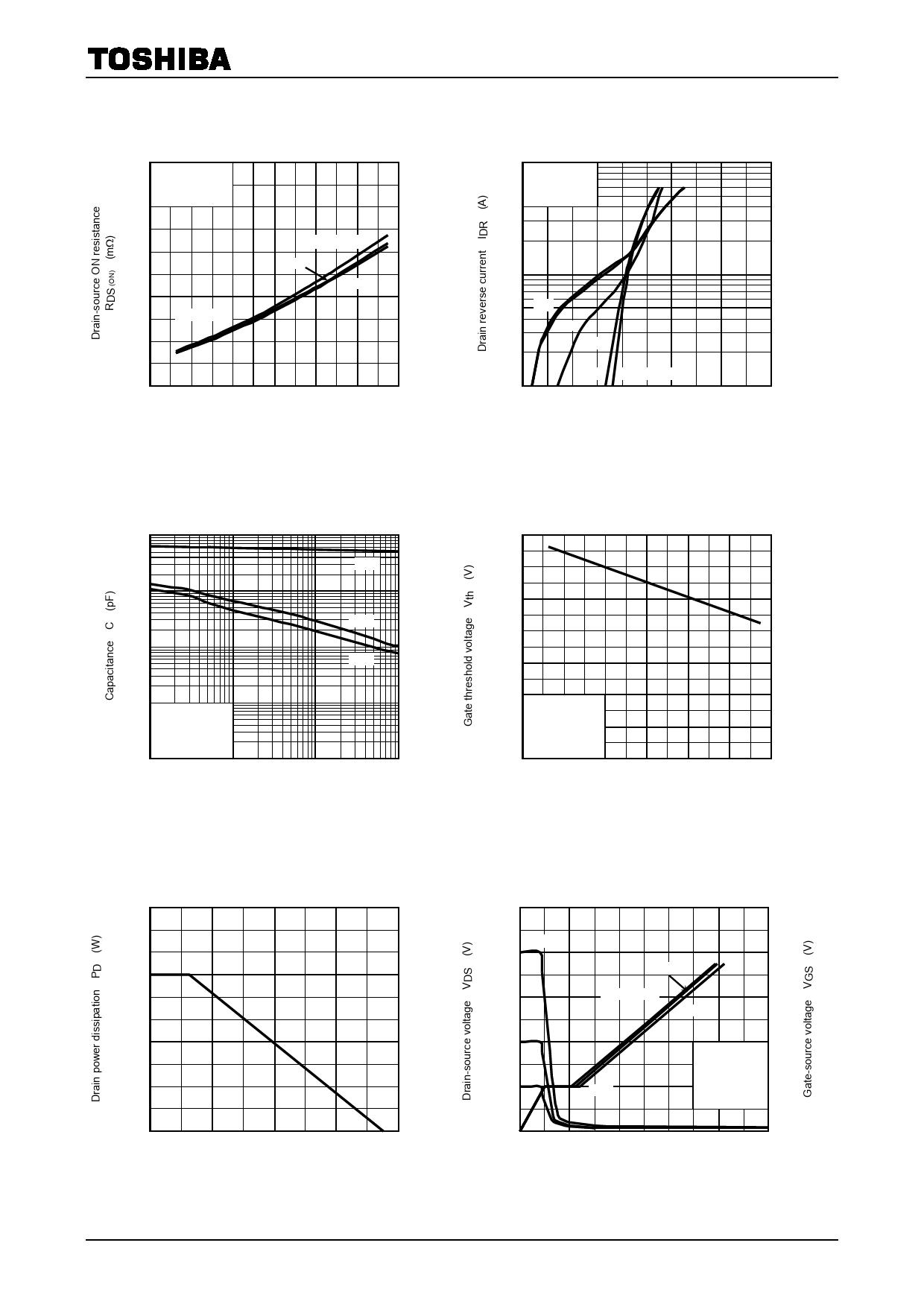
RDS (ON) − Tc
200
Common source
Pulse Test
160
120
80
VGS = −10 V
40
ID = −20 A
−10
−5
0
−80
−40
0
40
80
120
160
Case temperature Tc (°C)
TJ20A10M3
−100
Common source
Tc = 25°C
Pulse Test
IDR − VDS
−10
−10
−5
−3
−1 VGS = −0.1 V
−1
0
−0.4
−0.8
−1.2
−1.6
−2.0
Drain-source voltage VDS (V)
10000
1000
100
Capacitance – VDS
Ciss
Coss
Crss
10
Common source
VGS = 0 V
f =1MHz
Tc = 25°C
1
−0.1
−1
−10
Drain-source voltage VDS (V)
−100
Vth − Tc
−3.5
−3.0
−2.5
−2.0
−1.5
−1.0
Common source
−0.5
VDS = −10 V
ID = −1mA
Pulse Test
0
−80
−40
0
40
80
120
160
Case temperature Tc (°C)
PD − Tc
50
40
30
20
10
0
0
40
80
120
160
Case temperature Tc (°C)
−100
VDS
−80
−60
−40
−20
Dynamic input / output
characteristics
-20
-16
−40
VDD = −20 V
-12
−80
VGS
-8
Common source
ID = −20 A
Tc = 25°C
Pulse Test
-4
0
0
0
40
80
120
160
200
Total gate charge Qg (nC)
4
2018-06-01
Share Link: 