EV1HMC521ALC4(RevA) Просмотр технического описания (PDF) - Analog Devices
Номер в каталоге
Компоненты Описание
Список матч
EV1HMC521ALC4 Datasheet PDF : 24 Pages
| |||
Data Sheet
PIN CONFIGURATION AND FUNCTION DESCRIPTIONS
HMC521ALC4
NIC 1
NIC 2
GND 3
RF 4
GND 5
NIC 6
HMC521ALC4
TOP VIEW
(Not to Scale)
18 NIC
17 NIC
16 GND
15 LO
14 GND
13 NIC
NOTES
1. NIC = NOT INTERNALLY CONNECTED.
THESE PINS ARE NOT CONNECTED INTERNALLY.
2. EXPOSED PAD. THE EXPOSED PAD MUST BE
CONNECTED TO THE GND PIN.
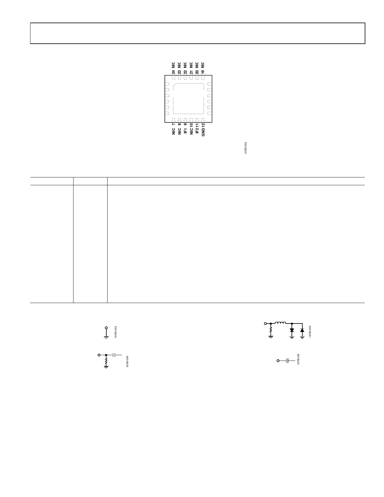
Figure 2. Pin Configuration
Table 4. Pin Function Descriptions
Pin No.
Mnemonic Description
1, 2, 6 to 8, NIC
10, 13,
17 to 24
Not Internally Connected. These pins are not connected internally.
3, 5, 12, 14, GND
16
Ground. These pins and package bottom must be connected to RF and dc ground. See Figure 3 for the GND
interface schematic.
4
RF
Radio Frequency Port. This pin is ac-coupled and matched to 50 Ω. See Figure 6 for the RF interface schematic.
9
IF2
Second Quadrature Intermediate Frequency Port. This pin is dc-coupled. For applications not requiring
operation to dc, dc block this port externally using a series capacitor of a value chosen to pass the necessary IF
frequency range. For operation to dc, these pins must not source or sink more than 2 mA of current. Otherwise,
die malfunction or die failure may result. See Figure 5 for the IFx interface schematic.
11
IF1
First Quadrature Intermediate Frequency Port. This pin is dc-coupled. For applications not requiring operation
to dc, dc block this port externally using a series capacitor of a value chosen to pass the necessary IF frequency
range. For operation to dc, these pins must not source or sink more than 2 mA of current. Otherwise, die
malfunction or die failure may result. See Figure 5 for the IFx interface schematic.
15
LO
Local Oscillator Port. This pin is ac-coupled and matched to 50 Ω. See Figure 4 for the LO interface schematic.
EPAD
Exposed Pad. The exposed pad must be connected to the GND pin.
INTERFACE SCHEMATICS
GND
IFx
Figure 3. GND Interface Schematic
LO
Figure 4. LO Interface Schematic
Figure 5. IFx Interface Schematic
RF
Figure 6. RF Interface Schematic
Rev. A | Page 5 of 24
Share Link: 