HMC520A(RevA) Просмотр технического описания (PDF) - Analog Devices
Номер в каталоге
Компоненты Описание
Список матч
HMC520A Datasheet PDF : 32 Pages
| |||
Data Sheet
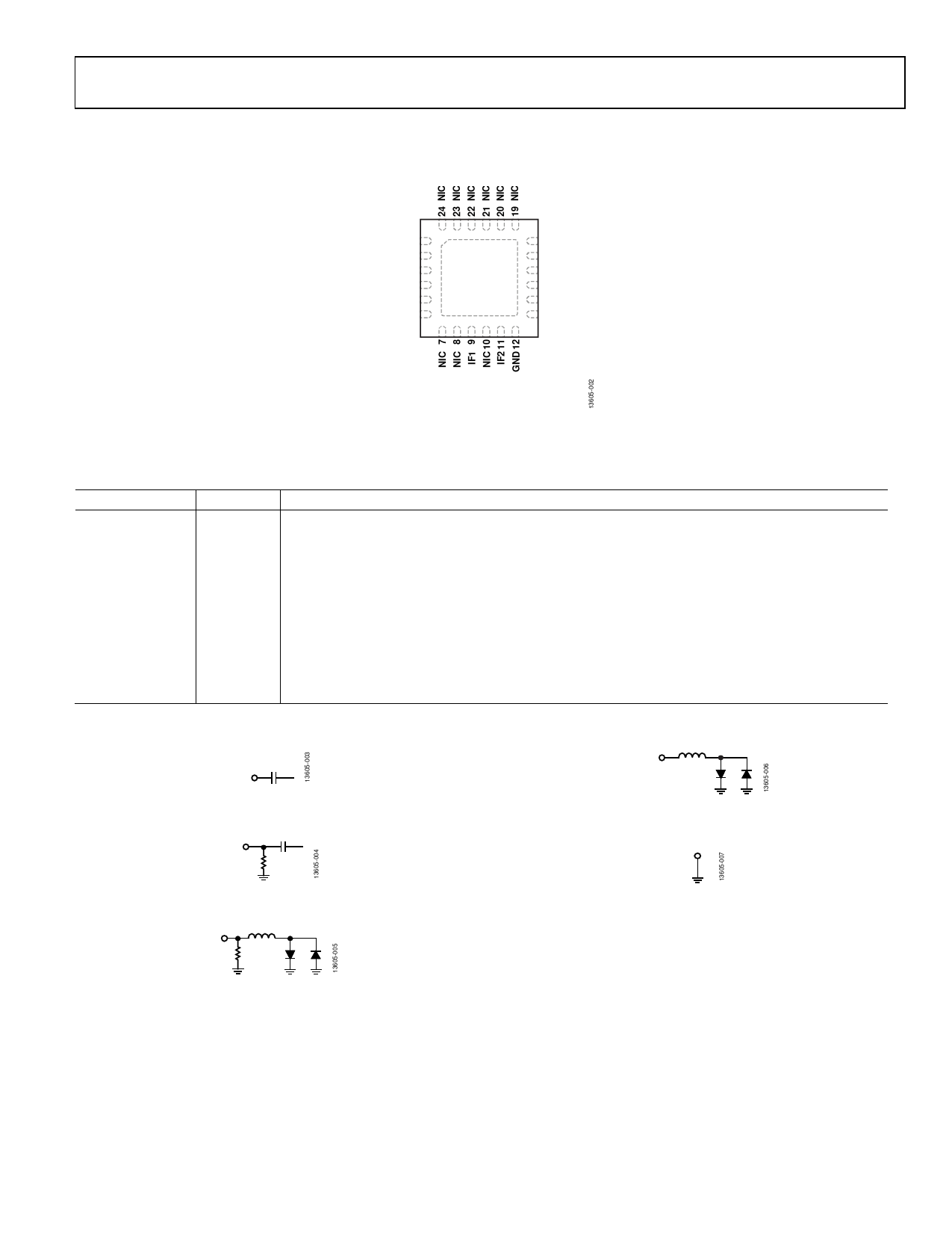
PIN CONFIGURATION AND FUNCTION DESCRIPTIONS
HMC520A
NIC 1
NIC 2
GND 3
RF 4
GND 5
NIC 6
HMC520A
TOP VIEW
(Not to Scale)
18 NIC
17 NIC
16 GND
15 LO
14 GND
13 NIC
NOTES
1. NIC = NOT INTERNALY CONNECTED.
2. EXPOSED PAD. THE EXPOSED PAD
MUST BE CONNECTED TO THE GND PIN.
Figure 2. Pin Configuration
Table 4. Pin Function Descriptions
Pin No.
Mnemonic Description
1, 2, 6 to 8, 10, 13, NIC
17 to 24
Not Internally Connected.
3, 5, 12, 14, 16
GND
Ground. See Figure 7 for the GND interface schematic.
4
RF
RF Port. This pin is ac-coupled internally and matched to 50 Ω. See Figure 3 for the RF interface schematic.
9, 11
IF1, IF2
First and Second Quadrature IF Input Pins. For applications that do not require operation to dc, use an
off chip dc blocking capacitor. For applications that require operation to dc, these pins must not
source or sink more than 12 mA of current because the device may not function or possible device
failure may result. See Figure 5 and Figure 6 for the IF1 and IF2 interface schematics.
15
LO
LO Port. This pin is dc-coupled and matched to 50 Ω. See Figure 4 for the LO interface schematic.
EPAD
Exposed Pad. The exposed pad must be connected to the GND pin.
INTERFACE SCHEMATICS
RF
Figure 3. RF Interface Schematic
LO
IF2
Figure 6. IF2 Interface Schematic
GND
Figure 4. LO Interface Schematic
IF1
Figure 7. GND Interface Schematic
Figure 5. IF1 Interface Schematic
Rev. A | Page 5 of 32
Share Link: 