HMC981 Просмотр технического описания (PDF) - Analog Devices
Номер в каталоге
Компоненты Описание
Список матч
HMC981 Datasheet PDF : 18 Pages
| |||
v00.0611
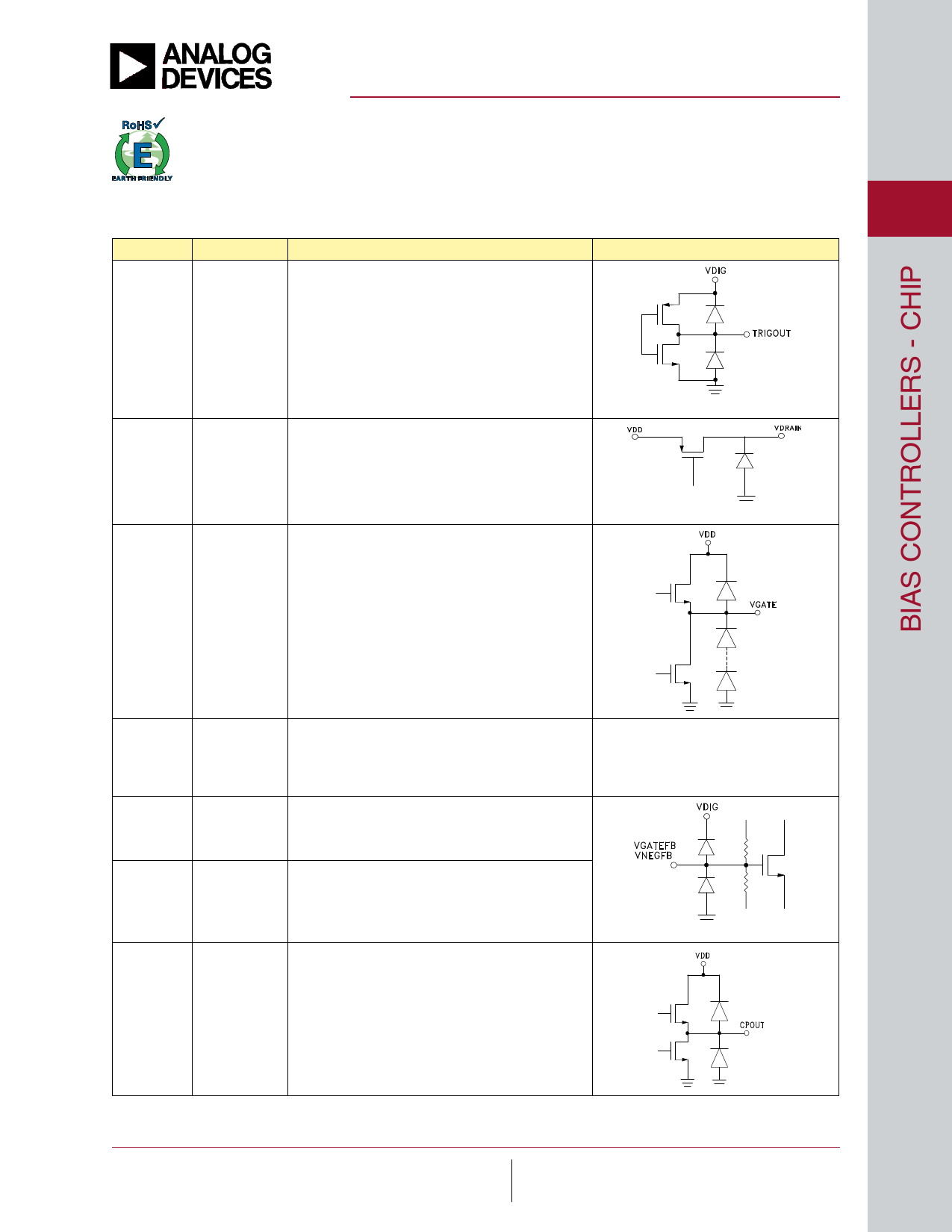
Pad Descriptions (Continued)
Pad Number
Function
Description
HMC981
ACTIVE BIAS CONTROLLER
Interface Schematic
Trigger out signal. Generates a HIGH (3.5V) signal when
14
TRGOUT
the active bias system stabilizes. This signal can be
used to trigger next device (ENABLE) if more than one
HMC981 is used in a daisy chain.
16, 17
VDRAIN
Drain voltage. Should be connected to the supply
terminal of the external amplifier. A minimum 100 nF
capacitor has to be placed close to the external amplifier to
improve load regulation.
Gate Control pad for external amplifier. Connect to the gate
(base) of the external amplifier. In order to guarantee
18
VGATE
stability,a 10μF capacitor should be connected between
the gate (base) terminal of the external amplifier and GND
as close to the amplifier as possible.
Negative input to the chip. Should be supplied with CPOUT
when negative voltage generator is enabled, or connect to
21
VNEG
external VSS when negative voltage generator is enabled.
For detailed usage please refer to the “Negative Voltage
Generator” section.
Feedback (Control) pad for Negative Voltage Generator
22
VNEGFB
Charge Pump. Float to activate the negative voltage
generator / Sort to GND to disable the negative voltage
generator.
Control pad for VGATEFB. Float VGATEFB when a
24
VGATEFB
depletion mode transistor is biased. Selects the mode of
operation along with VNEGFB pad. For detailed usage
please refer to the Table 2.
27, 28
CPOUT
Negative voltage generator charge pump output. Negative
voltage generator needs a flying capacitor, a reservoir
capacitor and two diodes to operate. Please refer to the
application schematic for more info.
IrnefsoFpromonarstiibopinlirtyfiucirsneais,shsedudmeebldyivbAeynAraylnoaglaoDgneDdveicvteicosesipsfolbareitlciseevuesdeo, rtnodorbefeorrsaac:ncyHuirnaifrtteitnigateenmdeMrnetlsiiacobfrlepo.awtHeonawtsveoevreorC,thneoorrp
rliicgehntsseofisthgirrdanptaerdtiebsythimatpmlicaaPytiorhensouonlrt ofertoh:me9rwit7sis8ues-eu2.ndS5ep0reca-inf3iyc3aptia4otne3sntsourbjpeFacttaetnoxt c:rhig9ahn7tgs8eowf-2Aithn5oau0lotg-n3oDti3ecve7i.c3eNso.
oFOornaretpTioreicnceh,,n2odleEolgilviyezrWayb,ayae,ntPdh.OtDo. rBpivolaxec9,e1C0oh6rd,eeNlrmos:rswAfoonoarddlo,,gMMADAe0v2i0c0e16s28,-29In410c.6,
POhrodnee:r7O81n-3-l2i9n-e47a0t0w• wOrwde.hr oitntliitnee.catowmww.analog.com
8
Trademarks and registered trademarks arAe tphepplriocpearttyioofntheSir urepsppecotivret:owPnehrso. ne: 978-250-3A3p4p3licaotrionaSpuppsp@orht:iPtthitoen.ec: o1-m800-ANALOG-D
Share Link: 