NJM2275F1 Просмотр технического описания (PDF) - Japan Radio Corporation
Номер в каталоге
Компоненты Описание
Список матч
NJM2275F1 Datasheet PDF : 11 Pages
| |||
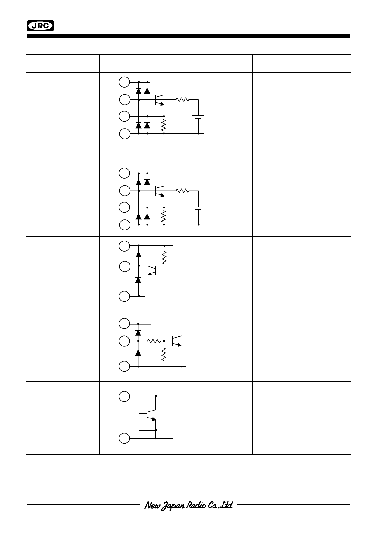
TERMINAL FUNCTION (Ta=25°C, V+=1.9 V)
Pin No. SYMBOL
EQUIVARENT CIRCUIT
6
1
1
RF IN
3
2
2k
500
2
GND
--
6
1
3
BIAS CAP
3
2
2k
500
6
5k
4
RF OUT
4
2
5
IREF
6
70
5
2
6
6
V+
2
NJM2275
VOLTAGE
FUNCTION
RF Input
1.09V
--
0.33V
Ground
Bias Capacitance
An external decoupling capacitor
is placed between this pin and
ground.
RF Output
V+
0.75V
--
Reference of Current Source
An external decoupling capacitor
is placed between this pin and
ground. An external resistor from
this pin to ground can controls the
reference current of current
source and the related
performances, such as NF and
gain.
Supply Voltage
ESD protection transistor exists
between V+ and ground.
Ver.2005-06-01
-6-
Share Link: 