W83194BR-KX Просмотр технического описания (PDF) - Winbond
Номер в каталоге
Компоненты Описание
Список матч
W83194BR-KX Datasheet PDF : 12 Pages
| |||
W83194BR-KX
PRELIMINARY
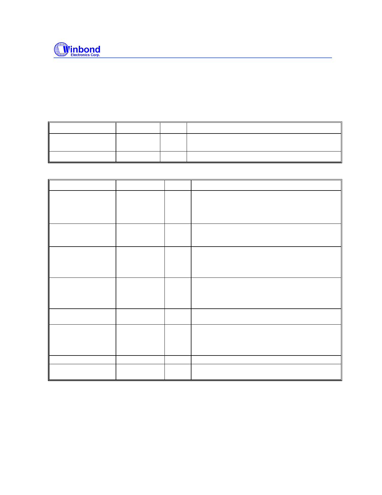
4.1 Crystal I/O
SYMBOL
Xin
Xout
PIN
I/O
FUNCTION
4
IN Crystal input with internal loading capacitors and
feedback resistors.
5
OUT Crystal output at 14.318MHz nominally.
4.2 CPU, SDRAM, PCI, IOAPIC Clock Outputs
SYMBOL
CPUT_CS
CPU_C0
CPU_T0
SDRAM [ 0 :12]
PCICLK0/
*MODE1
PCICLK1/*FS1
PCICLK [ 2 : 4 ]
PCICLK5/RESET#
BUFFER IN
*PD#
PIN
I/O
FUNCTION
46
OD CPU_C0 and CPU_T0 are the differential open drain
44
CPU clocks for K7. CPUT_CS is the open drain pin
43
for the chipset. It has the same phase relationship as
CPU_T0.
17,18,20,21,28,2
9,31,32,34,
35,37,38,40
7
8
10, 11,12
13
15
41
OUT
I/O
I/O
OUT
I/O
IN
IN
SDRAM clock outputs. Fanout buffer outputs from
BUFFER IN pin.(Controlled by chipset) They are
disabled when PD# is set LOW.
Free running PCI clock during normal operation.
Latched Input. Mode1=1, Pin 13 is PCICLK 5;
*Mode1=0, RESET# open drain. (4ms low active
pulse when Watch Dog time out)
Low skew (< 250ps) PCI clock outputs.
Latched input for FS1 at initial power up for H/W
selecting the output frequency of CPU, SDRAM and
PCI clocks.
Low skew (< 250ps) PCI clock outputs. Synchronous
to CPU clocks with 1-48ns skew (CPU early).
Low skew (< 250ps) PCI clock outputs.
Mode1=1, Pin 13 is PCICLK5; *Mode1=0, RESET#
open drain. (4ms low active pulse when Watch Dog
time out)
Inputs to fanout for SDRAM outputs.
The all clocks will be stopped when this pin set to
LOW.
Publication Release Date: May 2000
-3-
Revision 0.42
Share Link: 