CBT3245A Просмотр технического описания (PDF) - NXP Semiconductors.
Номер в каталоге
Компоненты Описание
Список матч
CBT3245A Datasheet PDF : 16 Pages
| |||
NXP Semiconductors
4. Functional diagram
A1 2
18 B1
CBT3245A
Octal bus switch
Fig 1. Logic diagram
5. Pinning information
5.1 Pinning
9
A8
19
OE
11 B8
001aao117
CBT3245A
n.c. 1
A1 2
A2 3
A3 4
A4 5
A5 6
A6 7
A7 8
A8 9
GND 10
CBT3245A
20 VCC
19 OE
18 B1
17 B2
16 B3
15 B4
14 B5
13 B6
12 B7
11 B8
aaa-001831
n.c. 1
A1 2
A2 3
A3 4
A4 5
A5 6
A6 7
A7 8
A8 9
GND 10
20 VCC
19 OE
18 B1
17 B2
16 B3
15 B4
14 B5
13 B6
12 B7
11 B8
aaa-001832
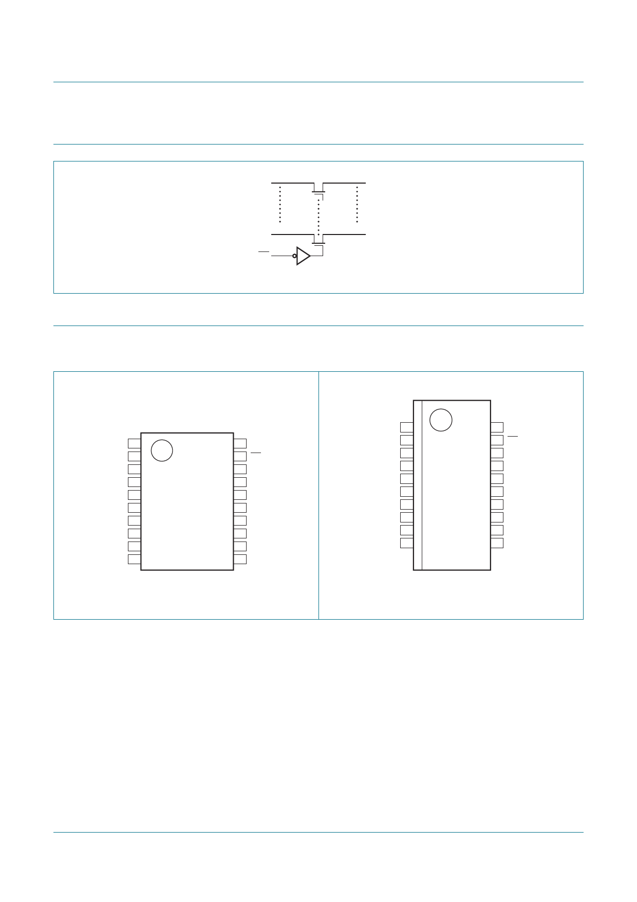
Fig 2. Pin configuration for SOT163-1 (SO20),
Fig 3. Pin configuration for SOT724-1 (SSOP20)
SOT339-1 (SSOP20) and SOT360-1 (TSSOP20)
CBT3245A
Product data sheet
All information provided in this document is subject to legal disclaimers.
Rev. 3 — 5 January 2012
© NXP B.V. 2012. All rights reserved.
2 of 16
Share Link: 