PI6C2305-1HW Просмотр технического описания (PDF) - Pericom Semiconductor Corporation
Номер в каталоге
Компоненты Описание
Список матч
PI6C2305-1HW Datasheet PDF : 6 Pages
| |||
PI6C2305-1
1122334455667788990011223344556677889900112233445566778899001122112233445566778899001122334455667788990011223344556677889900112211223344556677889900112233445566778899001122334455667788990011221122334455667788990011223344556677889900112233445566778899001122112233445566778899001122
3.3V Zero-Delay Buffer
Features
• Zero-input-output propagation delay
• 350ps phase error
• Multiple low-skew outputs
– Output-output skew less than 250ps
– Device-device skew less than 700ps
• 10 MHz to 100 MHz operating range
• Low Jitter <200ps
• High drive option (PI6C2305-1H)
• 3.3V operation
• Commercial Operation: 0°C to +70°C
• Industrial Operation: –40°C to +85°C
• Package: Space-saving 8-pin, 150-mil SOIC package (W)
Description
Providing five low-skew clocks, the PI6C2305-1 is a 3.3V zero-delay
buffer designed to distribute clock signals in applications including
PC, workstation, datacom, telecom, and high-performance systems.
The PI6C2305-1 provides 5 copies of clocks that have less than
350ps propagation delay compared to a reference clock. The skew
among the output clock signals for PI6C2305-1 is less than 250ps.
When there are no rising edges on the REF input, the PI6C2305-1
enters a power-down state. In this mode, the PLL is off and all outputs
are three-stated. This results in less than 50µA of current draw.
Featuring faster rise and fall times, the PI6C2305-1H is the high-drive
version of the PI6C2305-1.
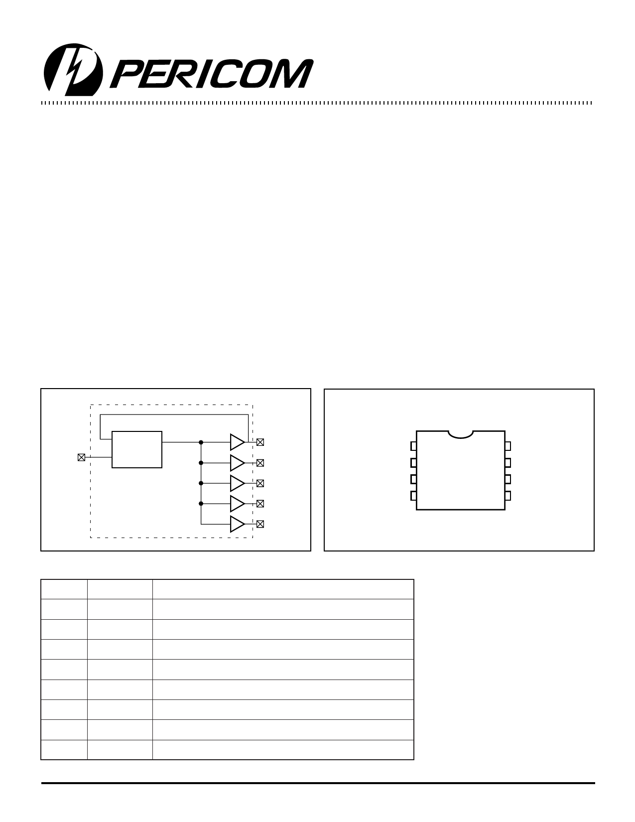
Block Diagram
Pin Configuration
FBK
REF
PLL
CLK0
CLK1
CLK2
CLK3
CLK4
REF 1
CLK2 2
CLK1 3
GND 4
8-Pin
W
8 CLK0
7 CLK4
6 VDD
5 CLK3
Pin Description
Pin
Signal
1
REF(1)
2
CLK2(2)
3
CLK1(2)
4
GND
5
CLK3(2)
6
VDD
7
CLK4(2)
8
CLK0(2)
Description
Input reference frequency, 5V Tolerant input
Buffered Clock output
Buffered Clock output
Ground
Buffered Clock output
3.3V Supply
Buffered Clock output
Buffered Clock output, internal feedback on this pin
1
Notes:
1. Weak pull-down.
2. Weak pull-down
on all outputs.
PS9477A
06/06/00
Share Link: 