SL23EP08 Просмотр технического описания (PDF) - Silicon Laboratories
Номер в каталоге
Компоненты Описание
Список матч
SL23EP08 Datasheet PDF : 15 Pages
| |||
SL23EP08
General Description-
Select Input Control-
The SL23EP08 is a low skew, low jitter Zero Delay Buffer
with very low operating current.
The product includes an on-chip high performance PLL that
locks into the input reference clock and produces nine (9)
output clock drivers tracking the input reference clock for
systems requiring clock distribution.
in addition to CLKOUT that is used for internal PLL
feedback, there are two (2) banks with four (4) outputs in
each bank, bringing the number of total available output
clocks to nine (9).
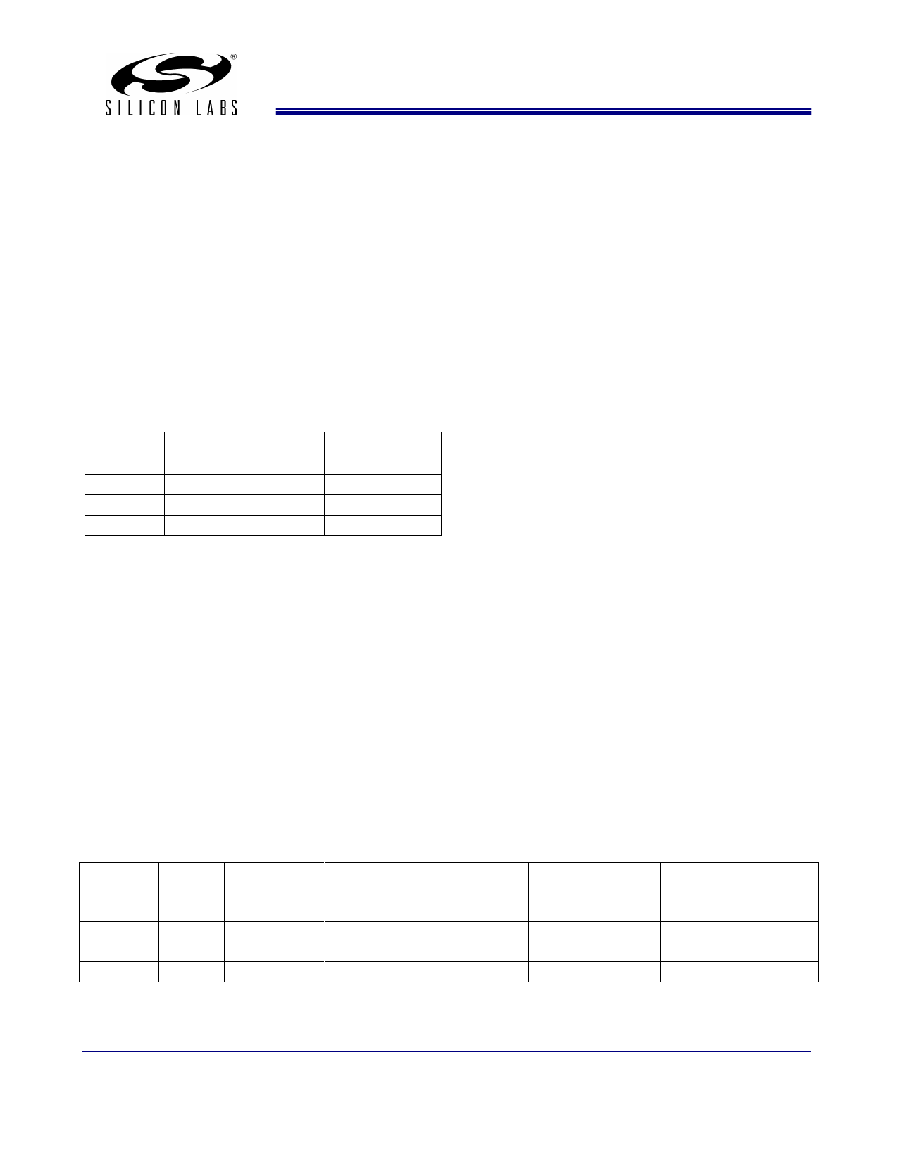
Input and output Frequency Range-
The input and output frequency range is the same. But, the
frequency range depends on VDD and drive levels as given
in the below Table 1.
VDD(V) Drive
Min(MHz) Max(MHz)
3.3
HIGH
10
220
3.3
STD
10
167
2.5
HIGH
10
200
2.5
STD
10
133
The SL23EP08 provides two (2) input select control pins
called S1 and S2. This feature enables users to selects
various states of output clock banks-A and bank-B, output
source and PLL shutdown features as shown in the Table 2.
The S1 (Pin-9) and S2 (Pin-8) inputs include 250 kΩ weak
pull-down resistors to GND.
PLL Bypass Mode
If the S1 and S2 pins are logic Low(0) and High(1)
respectively, the on-chip PLL is shutdown and bypassed,
and all the nine output clocks bank A, bank B and CLKOUT
clocks are driven by directly from the reference input clock.
In this operation mode SL23EP08 works like a non-ZDB
product.
High and Low-Drive Product Options -
The SL23EP08 is offered with High-Drive “-1H” and
Standard-Drive “-1” options. These drive options enable the
users to control load levels, frequency range and EMI
control. Refer to the AC electrical tables for the details.
Table 1. Input/Output Frequency Range
If the input clock frequency is less than 2 MHz or floating,
this is detected by an input frequency detection circuitry and
all eight (8) clock outputs are forced to Hi-Z. The PLL is
shutdown to save power. In this shutdown state, the product
draws less than 25 μA supply current.
SpreadThru™ Feature-
Skew and Zero Delay -
All outputs should drive the similar load to achieve output-to-
output skew and input-to-output specifications given in the
AC electrical tables. However, Zero delay between input and
outputs can be adjusted by changing the loading of CLKOUT
relative to the banks A and B clocks since CLKOUT is the
feedback to the PLL.
If a Spread Spectrum Clock (SSC) were to be used as an
input clock, the SL23EP08 is designed to pass the
modulated Spread Spectrum Clock (SSC) signal from its
reference input to the output clocks. The same spread
characteristics at the input are passed through the PLL and
drivers without any degradation in spread percent (%),
spread profile and modulation frequency
Power Supply Range (VDD)-
The SL23EP08 is designed to operate in a wide power
supply range from 2.3V (Min) to 3.3V (Max). An internal on-
chip voltage regulator is used to supply PLL constant power
supply of 1.8V, leading to a consistent and stable PLL
electrical performance in terms of skew, jitter and power
dissipation. Contact SLI for 1.8V power supply version ZDB
called SL23EPL08.
S2
0
0
1
1
S1
0
1
0
1
Clock A1-A4 Clock B1-B4 CLKOUT
Output Source
Tri-state
Driven
Driven[1]
Driven
Tri-state
Driven
Tri-state
Driven[1]
Driven
Driven (4)
Driven
Driven
Table 2. Select Input Decoding
PLL
PLL
Reference
PLL
PLL Shutdown and
Bypass
Yes
No
Yes
No
Rev 1.0, May 18, 2006
Page 3 of 15
Share Link: 