ADP3510ARU Просмотр технического описания (PDF) - Analog Devices
Номер в каталоге
Компоненты Описание
Список матч
ADP3510ARU Datasheet PDF : 16 Pages
| |||
ADP3510
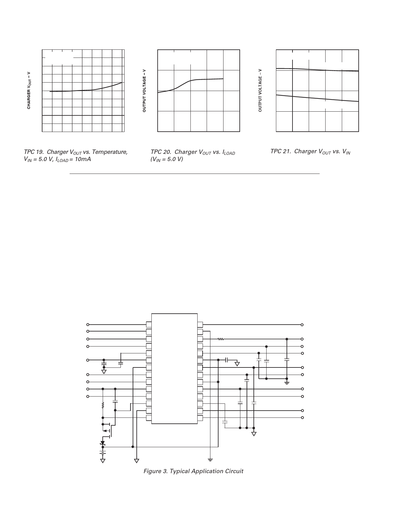
4.25
4.24
4.23
VIN = 5.0V
ILOAD = 10mA
4.22
4.21
4.20
4.19
4.18
4.17
4.16
4.15
–40 –20
0 20 40 60 80
TEMPERATURE – ؇C
100 120
TPC 19. Charger VOUT vs. Temperature,
VIN = 5.0 V, ILOAD = 10mA
4.22
VIN = 5V
RSENSE = 250m⍀
4.21
4.20
4.19
4.18
0
200
400
600
800 1000
ILOAD – mA
TPC 20. Charger VOUT vs. ILOAD
(VIN = 5.0 V)
4.210
RSENSE = 250m⍀
4.205
ILOAD = 500mA
4.200
4.195
ILOAD = 10mA
4.190
5
6
7
8
9
10
INPUT VOLTAGE – V
TPC 21. Charger VOUT vs. VIN
THEORY OF OPERATION
The ADP3510 is a total solution power management chip for use
with CDMA baseband chipsets and is optimized for the CBP3.0/
4.0 type chipsets. Figure 1 shows a block diagram of the ADP3510.
The ADP3510 contains several blocks:
∑ Six Low Dropout Regulators (Input-Output, Core, Analog,
Crystal Oscillator, Memory, Realtime Clock)
∑ Reset Generator
∑ Buffered Precision Reference
∑ Lithium Ion Charge Controller and Processor Interface
∑ Power-On/-Off Logic
∑ Undervoltage Lockout
∑ Deep Discharge Lockout
These functions have traditionally been done either as a discrete
implementation or as a custom ASIC design. The ADP3510
combines the benefits of both worlds by providing an integrated
standard product where every block is optimized to operate in a
CDMA environment while maintaining a cost-competitive solution.
Figure 3 shows the external circuitry associated with the ADP3510.
Only a minimal number of support components are required.
Input Voltage
The input voltage range of the ADP3510 is 3.2 V to 7.5 V and is
optimized for a single Li-Ion cell or three NiMH cells. The thermal
impedance of the ADP3510 is 68∞C/W for four layer boards. The
end of charge voltage for high capacity NiMH cells can be as high
as 5.5 V. Power dissipation should be calculated at maximum ambi-
ent temperatures and battery voltage in order not to exceed the 125∞C
maximum allowable junction temperature. Figure 4 shows the maxi-
mum power dissipation as a function of ambient temperature.
PWRON
PWRONKEY
KEYPADROW
ALARM
VRTC
C1
0.1F
ADC
GPIO
CHARGER IN
GPIO
R1
0.25⍀
C2
10nF
C3
1.0nF
Q1
SI3441DY
D1
10BQ015
Li؉
BATTERY
ADP3510
1 PWRONIN TCXOEN 28
2 PWRONKEY AGND 27
3 ROWX
REFOUT 26
4 ALARM
VTCXO 25
5 PDCAP
VAN 24
6 VRTC
VBAT 23
7 BATSNS
VCORE 22
8 MVBAT
VMEM 21
9 CHRDET
VBAT2 20
10 CHRIN
VIO 19
11 GATEIN
RESET 18
12 GATEDR RESCAP 17
13 DGND
CHGEN 16
14 ISENSE
EOC 15
TCXOEN
R2 10⍀
C4
10F
C9
2.2F
C7
2.2F
C10
0.22F
C6
2.2F
C5
0.1F
C8
2.2F
C11
0.1F
REF
VTCXO
VAN
VCORE
VMEM
VIO
RESET
GPIO
GPIO
Figure 3. Typical Application Circuit
–10–
REV. 0
Share Link: 