CY7C1041CV33 Просмотр технического описания (PDF) - Cypress Semiconductor
Номер в каталоге
Компоненты Описание
Список матч
CY7C1041CV33 Datasheet PDF : 12 Pages
| |||
CY7C1041CV33
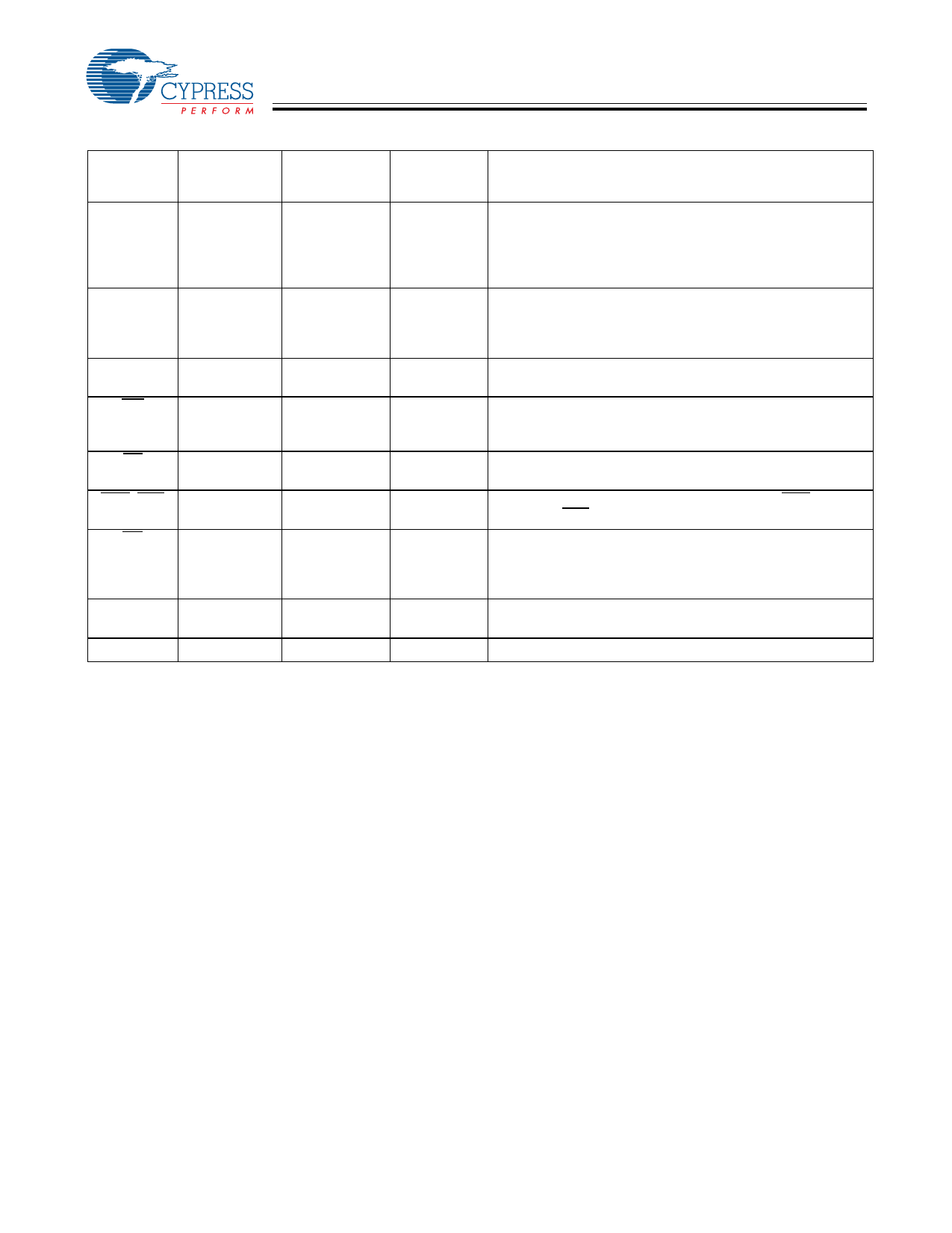
Pin Definitions
Pin Name
A0–A17
I/O0–I/O15
NC
WE
CE
BHE, BLE
OE
VSS
VCC
44-SOJ,
44-TSOP
Pin Number
48-ball FBGA
Pin Number
I/O Type
Description
1–5, 18–27,
42–44
A3, A4, A5, B3,
B4, C3, C4, D4,
H2, H3, H4, H5,
G3, G4, F3, F4,
E4, D3
Input
Address Inputs used to select one of the address
locations.
7–10,13–16,
29–32, 35–38
B1, C1, C2, D2,
E2, F2, F1, G1,
B6, C6, C5, D5,
E5, F5, F6, G6
Input/Output Bidirectional Data I/O lines. Used as input or output lines
depending on operation
28
A6, E3, G2, H1, No Connect No Connects. This pin is not connected to the die
H6
17
G5
Input/Control Write Enable Input, active LOW. When selected LOW, a
WRITE is conducted. When selected HIGH, a READ is
conducted.
6
B5
Input/Control Chip Enable Input, active LOW. When LOW, selects the chip.
When HIGH, deselects the chip.
40, 39
41
B2, A1
A2
Input/Control
Input/Control
Byte Write Select Inputs, active LOW. BHE controls
I/O15–I/O8, BLE controls I/O7–I/O0
Output Enable, active LOW. Controls the direction of the I/O
pins. When LOW, the I/O pins are allowed to behave as
outputs. When deasserted HIGH, I/O pins are tri-stated, and
act as input data pins.
12, 34
D1, E6
Ground
Ground for the device. Should be connected to ground of the
system.
11, 33
D6, E1
Power Supply Power Supply inputs to the device.
Document #: 38-05134 Rev. *H
Page 3 of 12
[+] Feedback
Share Link: 