HTG12N0 Просмотр технического описания (PDF) - Holtek Semiconductor
Номер в каталоге
Компоненты Описание
Список матч
HTG12N0 Datasheet PDF : 30 Pages
| |||
HTG12N0
Functional Description
Program counter – PC
This counter addresses the program ROM and
is arranged as a 12-bit binary counter from PC0
to PC11 whose contents specify a maximum of 4096
addresses. The program counter counts with an in-
crement of 1 or 2 with each execution of an instruction.
When executing the jump instruction (JMP,
JNZ, JC, JTMR,...), a subroutine call, initial
reset, internal interrupt, RTC interrupt or re-
turning from a subroutine, the program counter
is loaded with the corresponding instruction
data as shown in the table.
Notes: P0~P11: Instruction code
@: PC11 keeps the current value
S0~S11: Stack register bits
PB0 and PB1 are set to 0 at power on
reset.
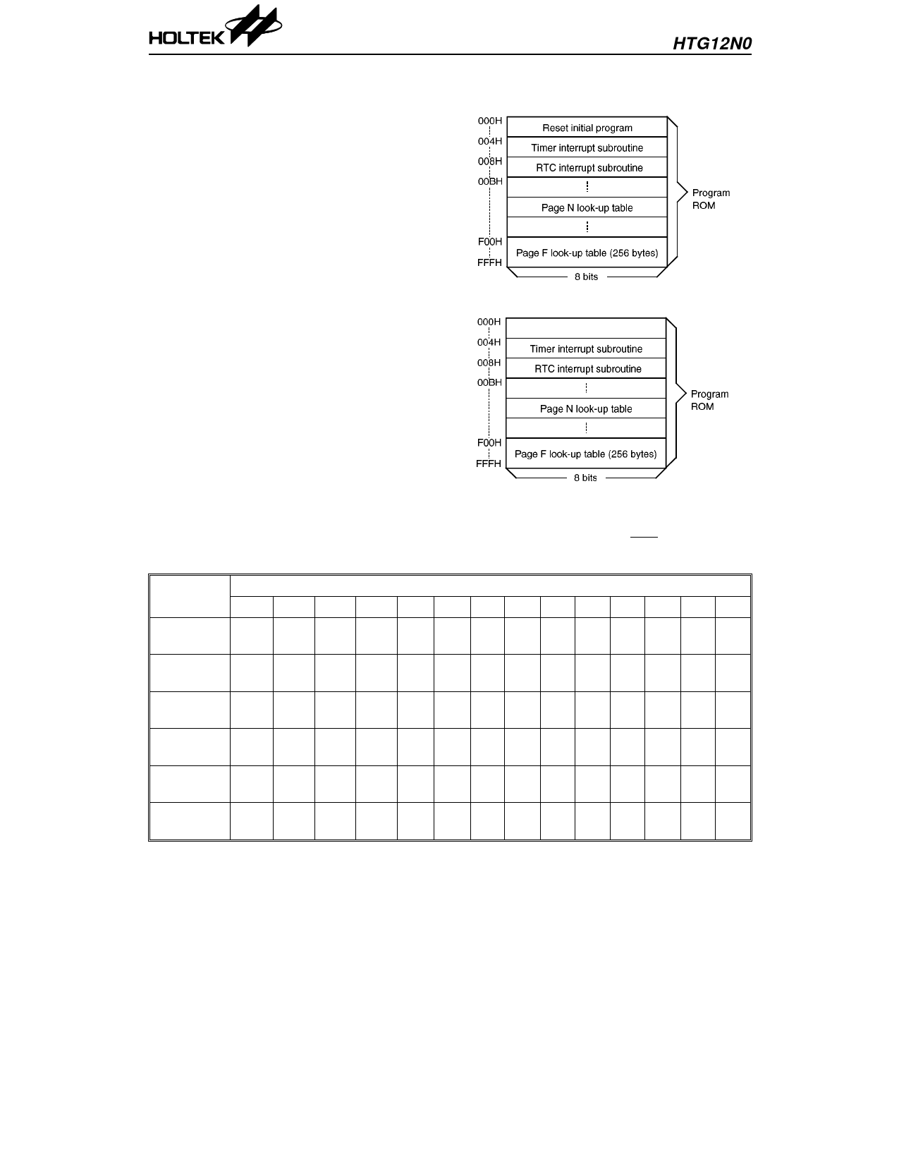
Program memory PB0=0, PB1=0
Program memory – ROM
The program memory is the executable memory
and is arranged in a 4096×8 bit format. There are
four banks for the program memory in HTG12N0,
each bank shown in the figure can be switched by
the assignment of PB0 and PB1. The address is
specified by the program counter (PC). Four spe-
cial locations are reserved as shown below.
Program memory PB0=1, PB1=0
• Location 0
Activating the processor RES pin causes the
first instruction to be fetched from location 0.
Mode
Program Counter
PC13 PC12 PC11 PC10 PC9 PC8 PC7 PC6 PC5 PC4 PC3 PC2 PC1 PC0
Initial
reset
PB1 PB0 0
0
0 000000000
Internal
interrupt
PB1 PB0 0
0
0 000000100
External
interrupt
PB1 PB0 0
0
0 000001000
Jump, call
instruction
PB1
PB0
P11
P10
P9
P8
P7
P6
P5
P4
P3
P2
P1 P0
Conditional
branch
PB1
PB0
@
P10 P9 P8 P7 P6 P5 P4 P3 P2 P1 P0
Return from
subroutine
PB1
PB0
S11
S10
S9
S8
S7 S6
S5
S4
S3
S2
S1
S0
Program memory
8
18th Mar ’99
Share Link: 