CMX264D5 Просмотр технического описания (PDF) - CML Microcircuits
Номер в каталоге
Компоненты Описание
Список матч
CMX264D5 Datasheet PDF : 25 Pages
| |||
Frequency Domain Split Band Scrambler
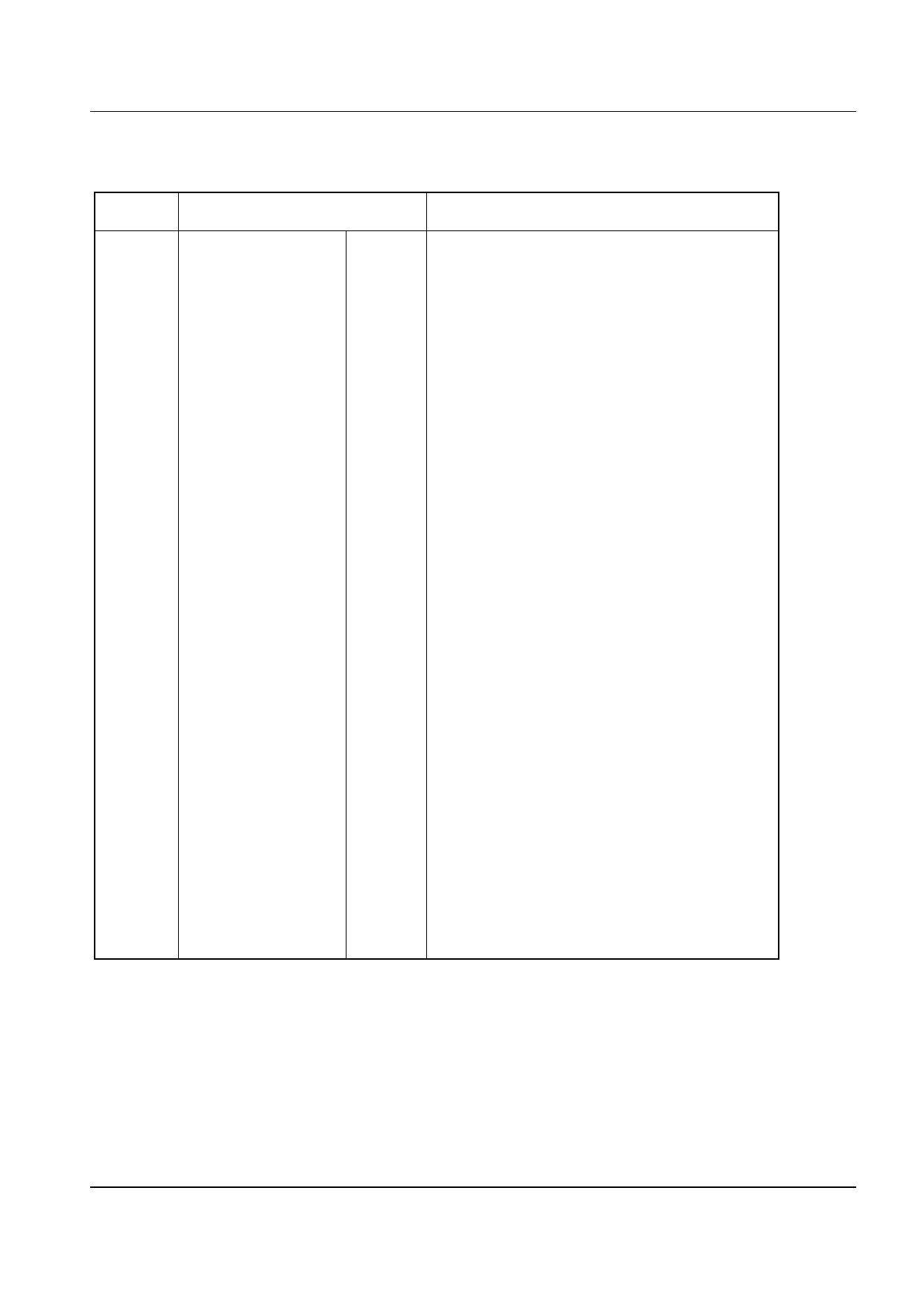
1.3 Signal List (continued)
CMX264
Package
D5
Signal
Pin No.
Name
15
-
16
MUTERX
17
EXTO
18
-
19
RECO
20
-
21
CSN
22
SCLOCK
23
SDATA
24
VDD
Description
Type
-
This pin should be left unconnected.
I/P A logic input which when high (VDD) immediately
de-activates the two Rx outputs (RECO and
EXTO), overriding the serial data previously
loaded. When this input is low (VSS), the Rx
outputs are controlled by the serial data port.
O/P One of two Rx outputs. This is used for routeing
the recovered audio to external devices, e.g. a
speakerphone. This output may be
independently activated or de-activated by
selecting the appropriate internal state. When
de-activated, either by the serial data or by the
MUTERX pin, the output is set to VBIAS.
-
This pin should be left unconnected.
O/P The other Rx output. This is used for routeing
the recovered audio to the telephone
loudspeaker. This output may be independently
activated or de-activated by selecting the
appropriate internal state. When de-activated,
either by the serial data or by the MUTERX pin,
the output is set to VBIAS.
-
This pin should be left unconnected.
I/P )The serial port input pins. Data applied here
I/P )sets up the internal state of the device, e.g. split
I/P )point, scramble/clear, etc. See Figure 10.
POWER
The positive supply rail. This pin must be
decoupled to VSS by a capacitor mounted close
to the device.
Notes: I/P = Input
O/P = Output
BI = Bidirectional
© 1999 Consumer Microcircuits Limited
5
D/CMX264/1
Share Link: 