HTG12G0 Просмотр технического описания (PDF) - Holtek Semiconductor
Номер в каталоге
Компоненты Описание
Список матч
HTG12G0 Datasheet PDF : 31 Pages
| |||
HTG12G0
Working registers – R0, R1, R2, R3, R4
These five registers are usually used to store the
frequently accessed data. The working register
can be incremented (+1) or decremented (–1).
The JNZ Rn,address (n=0,1,4) instruction
makes very efficient use of the working register
as program loop counter. The register pairs of
R1, R0 and R3, R2 can also be used as the data
memory pointer, when the data memory trans-
fer instruction is executed.
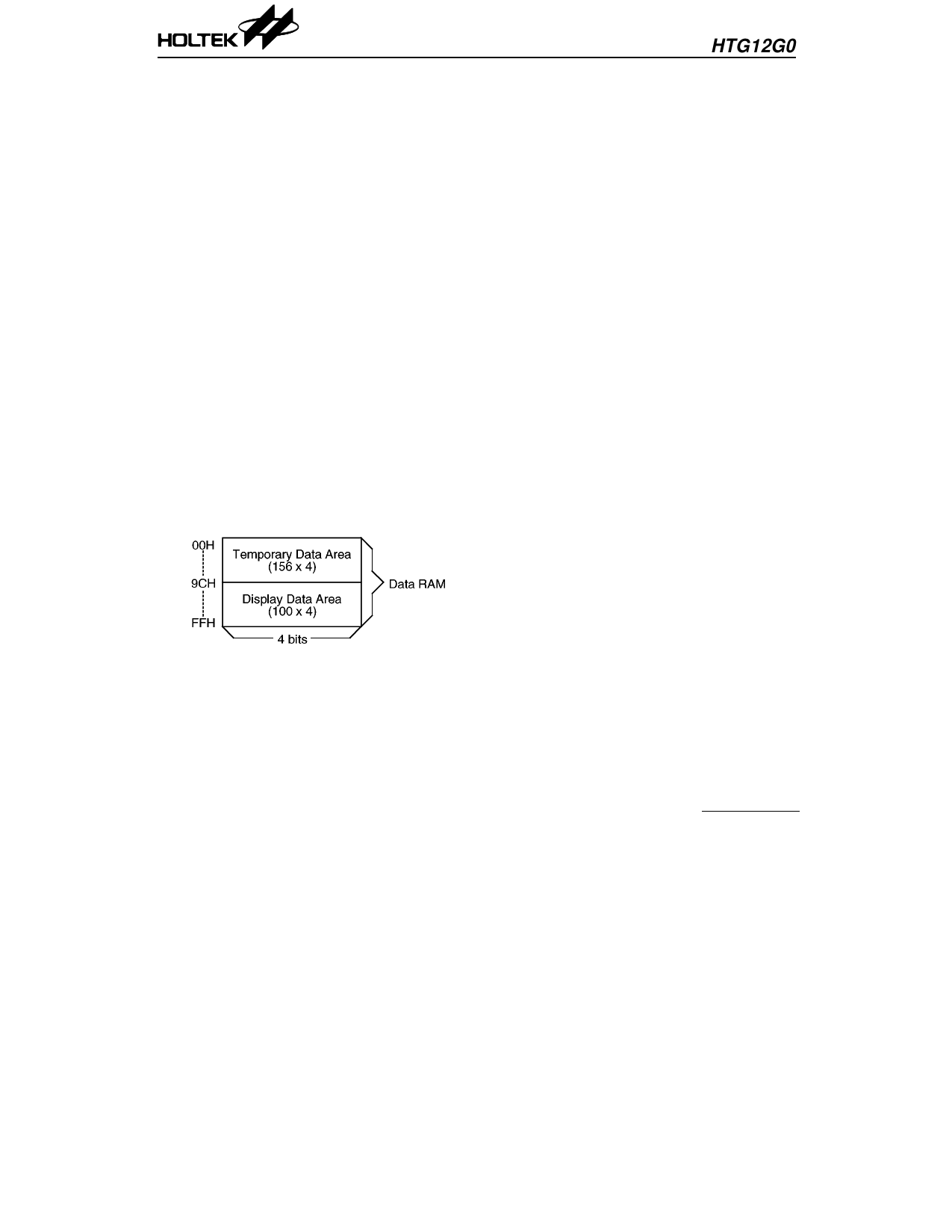
Data memory – RAM
The data memory is a static RAM organized
with 256 × 4 bits and is used to store temporary
data and display data. All of the data memory
locations are indirectly addressable through the
register pair “R1, R0” or “R3, R2”.
There are two areas in the data memory, tempo-
rary data area and display data area. Access to
temporary data memory is made through
00H~9BH address, and access to display data
memory is made in 9CH~FFH address.
When data is written in the display area, the
LCD driver automatically reads it and gene-
rates an LCD driving signal.
Data memory
Accumulator – ACC
The register ACC plays the most important role
in data manipulation and data transfer. It is not
only one of the sources of input to the ALU but
also the destination of the result due to ALU.
Data transfer can be performed between ACC
and other registers, data memory or I/O ports.
Arithmetic and logic unit – ALU
This circuit performs arithmetic and logic op-
eration. The ALU provides the following func-
tions:
• Arithmetic operation
(ADD, ADC, SUB, SBC, DAA)
• Logic operation (AND, OR, XOR)
• Rotation (RL, RR, RLC, RRC)
• Increment and Decrement (INC, DEC)
• Branch decision (JZ, JNZ, JC, JNC...)
The ALU not only outputs the results of data
operation but also sets the status of carry flag
(C) in some instructions.
Timer
This is a programmable 8–bit count-up counter,
internal frequency sources used to aid the user
in counting and generating accurate time base.
The Timer can be pre-set and read with soft-
ware instructions. “TIMER XXH”, “MOV
TMRL, A” and “MOV TMRH, A” preload TIMER
value. “MOV A, TMRL” and “MOV A, TMRH”
read the contents of TIMER to ACC.
The Timer is stopped by a hardware reset or
“TIMER OFF” instruction and started by a
TIMER ON instruction.
Once the Timer is started, it will increment to
its maximum count (FFH) and overflows to zero
(00H). It will not stop until there is a “TIMER
OFF” instruction or reset. When an overflow
occurs, it will set the Timer Flag (TF) simulta-
neously. If interrupt is enabled, the Timer cir-
cuit supports TF for internal interrupt. The
state of the TF can be tested with the condi-
tional instruction JTMR.
The Timer flag is cleared after the interrupt or
JTMR instruction is executed.
The frequency of the internal frequency source
can be selected by mask option.
Frequency of TIMER clock =
system clock
2n
Where n=0,1,2......13 except 6, by mask option
(the sixth stage is reserved for internal use).
10
14th May ’99
Share Link: 