74HC280D Просмотр технического описания (PDF) - NXP Semiconductors.
Номер в каталоге
Компоненты Описание
Список матч
74HC280D Datasheet PDF : 15 Pages
| |||
Nexperia
74HC280; 74HCT280
9-bit odd/even parity generator/checker
Table 7. Dynamic characteristics …continued
Voltages are referenced to GND (ground = 0 V); CL = 50 pF unless otherwise specified; for test circuit, see Figure 6.
Symbol Parameter Conditions
25 C
40 C to +85 C 40 C to +125 C Unit
Min Typ Max Min Max Min Max
74HCT280
tpd
propagation In to PE; see Figure 5
delay
VCC = 4.5 V
[1]
- 21 42
-
53
-
63 ns
VCC = 5.0 V; CL = 15 pF
- 18 -
-
-
-
- ns
In to PO; see Figure 5
VCC = 4.5 V
- 26 45
-
56
-
68 ns
VCC = 5.0 V; CL = 15 pF
- 22 -
-
-
-
- ns
tt
transition see Figure 5
time
VCC = 4.5 V
[2]
- 7 15
-
19
-
22 ns
CPD
power
per package;
dissipation VI = GND to VCC 1.5 V
capacitance
[3] -
65
-
-
-
-
- pF
[1] tpd is the same as tPHL and tPLH.
[2] tt is the same as tTHL and tTLH.
[3] CPD is used to determine the dynamic power dissipation (PD in W):
PD = CPD VCC2 fi N + (CL VCC2 fo) where:
fi = input frequency in MHz;
fo = output frequency in MHz;
CL = output load capacitance in pF;
VCC = supply voltage in V;
N = number of inputs switching;
(CL VCC2 fo) = sum of outputs.
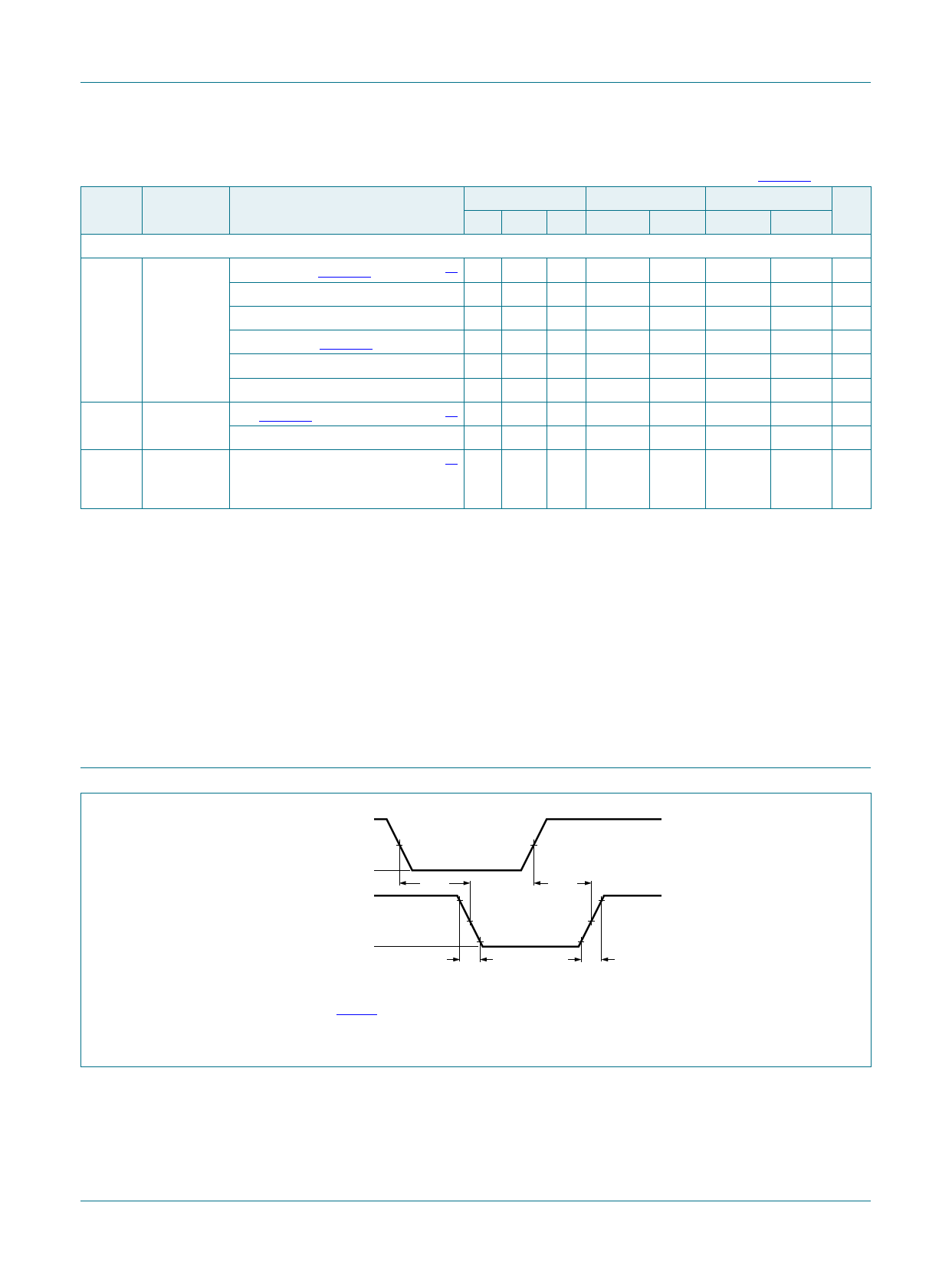
11. Waveforms
9,
,QLQSXW
*1'
92+
3(32RXWSXW
92/
90
W3+/
9<
W7+/
90
9;
W3/+
W7/+
DDD
Fig 5.
Measurement points are given in Table 8.
VOL and VOH are typical voltage output levels that occur with the output load.
Input (In) to output (PE, PO) propagation delays and output transition times
74HC_HCT280
Product data sheet
All information provided in this document is subject to legal disclaimers.
Rev. 3 — 15 September 2016
.
7 of 15
© Nexperia B.V. 2017. All rights reserved
Share Link: 