74ABT544PW,118 Просмотр технического описания (PDF) - NXP Semiconductors.
Номер в каталоге
Компоненты Описание
Список матч
74ABT544PW,118 Datasheet PDF : 17 Pages
| |||
NXP Semiconductors
74ABT544
Octal latched transceiver with dual enable; 3-state
Table 7. Dynamic characteristics …continued
GND = 0 V; for test circuit, see Figure 10.
Symbol Parameter
Conditions
tPHL
tPZH
tPZL
tPHZ
tPLZ
tsu(H)
tsu(L)
th(H)
th(L)
tWL
HIGH to LOW
An to Bn or Bn to An; see Figure 5
propagation delay LEBA to An or LEAB to Bn; see Figure 6
OFF-state to HIGH OEBA to An, OEAB to Bn; see Figure 7
propagation delay EBA to An, EAB to Bn; see Figure 7
OFF-state to LOW OEBA to An, OEAB to Bn; see Figure 8
propagation delay EBA to An, EAB to Bn; see Figure 8
HIGH to OFF-state OEBA to An, OEAB to Bn; see Figure 7
propagation delay EBA to An, EAB to Bn; see Figure 7
LOW to OFF-state OEBA to An, OEAB to Bn; see Figure 8
propagation delay EBA to An, EAB to Bn; see Figure 8
set-up time HIGH An to LEAB, Bn to LEBA; see Figure 9
An to EAB, Bn to EBA; see Figure 9
set-up time LOW An to LEAB, Bn to LEBA; see Figure 9
An to EAB, Bn to EBA; see Figure 9
hold time HIGH
LEAB to An, LEBA to Bn; see Figure 9
EAB to An, EBA to Bn; see Figure 9
hold time LOW
LEAB to An, LEBA to Bn; see Figure 9
EAB to An, EBA to Bn; see Figure 9
pulse width LOW latch enable; see Figure 9
11. Waveforms
25 C; VCC = 5.0 V 40 C to +85 C; Unit
VCC = 5.0 V 0.5 V
Min Typ Max Min
Max
2.4 3.6 4.5 2.4
5.2 ns
3.0 4.4 5.3 3.0
6.2 ns
1.8 3.0 3.9 1.8
4.7 ns
1.9 3.4 4.1 1.9
5.0 ns
2.9 4.2 5.2 2.9
6.1 ns
3.1 4.6 5.5 3.1
6.5 ns
2.0 3.3 4.3 2.0
4.9 ns
2.1 3.4 4.5 2.1
5.2 ns
2.0 2.8 5.8 2.0
6.3 ns
2.0 3.0 6.2 2.0
6.7 ns
3.0 1.5 -
3.0
- ns
3.0 1.5 -
3.0
- ns
3.0 0.6 -
3.0
- ns
3.0 0.6 -
3.0
- ns
+0.5 0.3 -
0.5
- ns
+0.5 0.2 -
0.5
- ns
+0.5 1.3 -
0.5
- ns
+0.5 1.3 -
0.5
- ns
3.5 1.8 -
3.5
- ns
VI
An, Bn
GND
VOH
Bn, An
VOL
VM
VM
tPHL
tPLH
VM
VM
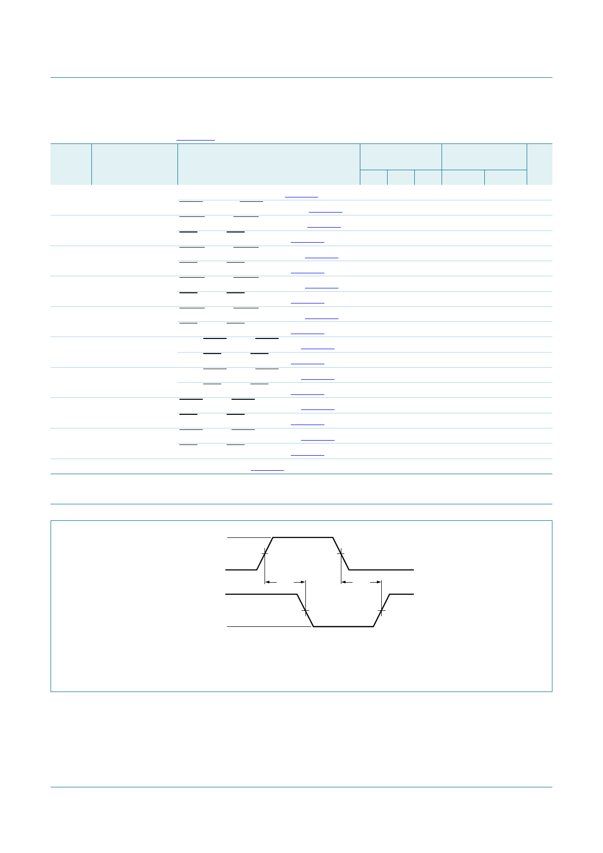
001aac759
Fig 5.
VM = 1.5 V
VOL and VOH are typical voltage output levels that occur with the output load.
Propagation delay input (An, Bn) to output (Bn, An)
74ABT544
Product data sheet
All information provided in this document is subject to legal disclaimers.
Rev. 6 — 3 November 2011
© NXP B.V. 2011. All rights reserved.
7 of 16
Share Link: 