74ABT544PW,118 Просмотр технического описания (PDF) - NXP Semiconductors.
Номер в каталоге
Компоненты Описание
Список матч
74ABT544PW,118 Datasheet PDF : 17 Pages
| |||
NXP Semiconductors
74ABT544
Octal latched transceiver with dual enable; 3-state
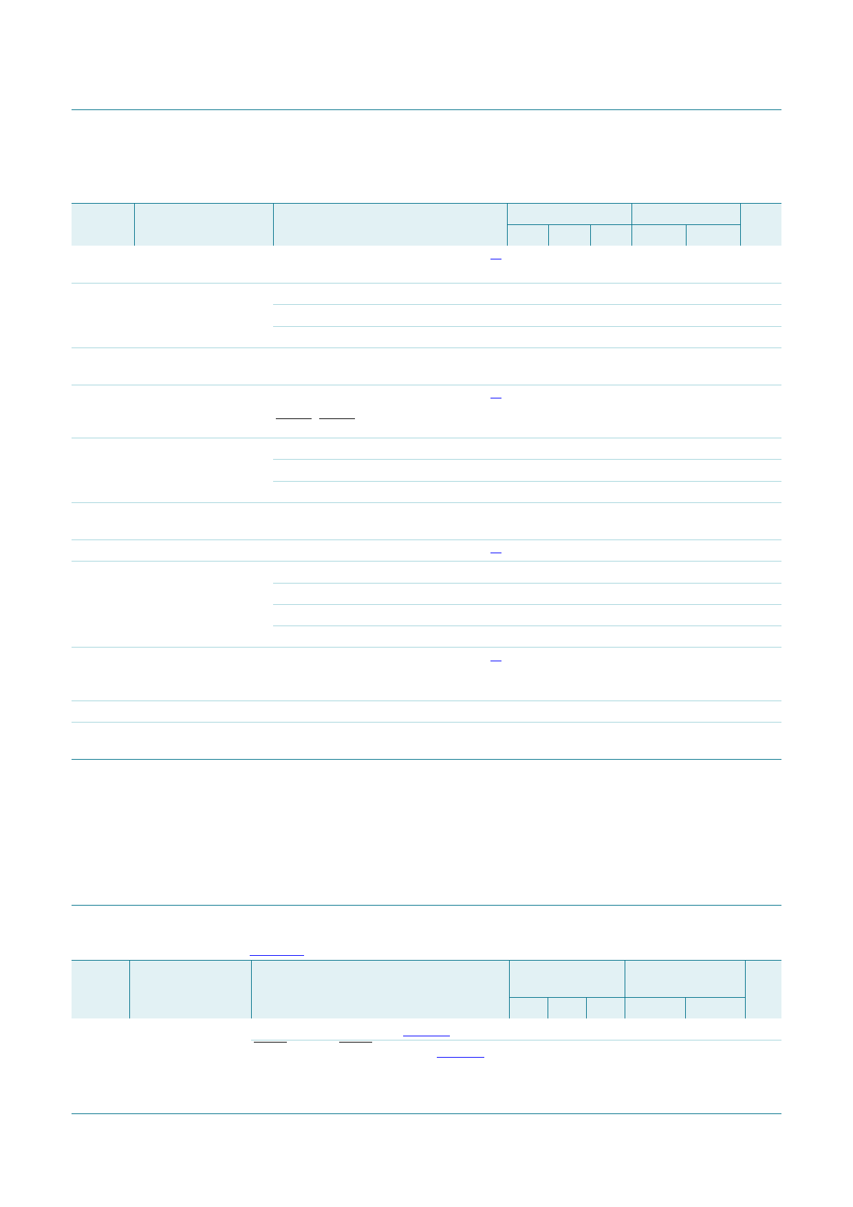
Table 6. Static characteristics …continued
Voltages are referenced to GND (ground = 0 V).
Symbol Parameter
Conditions
VOL(pu)
II
IOFF
IO(pu/pd)
IOZ
ILO
IO
ICC
ICC
CI
CI/O
power-up LOW-level
output voltage
input leakage current
VCC = 5.5 V; IO = 1 mA;
VI = GND or VCC
VCC = 5.5 V; VI = GND or 5.5 V
control pins
An, Bn
power-off leakage
current
VCC = 0 V; VI or VO 4.5 V
power-up/power-down VCC = 2.1 V; VO = 0.5 V;
output current
VI = GND or VCC;
OEAB, OEBA don’t care
OFF-state output
current
VCC = 5.5 V; VI = VIL or VIH
VO = 2.7 V
VO = 0.5 V
output leakage current HIGH-state; VO = 5.5 V;
VCC = 5.5 V; VI = GND or VCC
output current
VCC = 5.5 V; VO = 2.5 V
supply current
VCC = 5.5 V; VI = GND or VCC
outputs HIGH-state
outputs LOW-state
outputs disabled
additional supply
current
per input pin; VCC = 5.5 V; one input
pin at 3.4 V, other inputs at VCC or
GND
input capacitance
input/output
capacitance
VI = 0 V or VCC
outputs disabled; VO = 0 V or VCC
25 C
40 C to +85 C Unit
Min Typ Max Min Max
[1] - 0.13 0.55
-
0.55 V
- 0.01 1.0
-
- 5.0 100 -
- 5.0 100 -
[2] - 5.0 50
-
1.0 A
100 A
100 A
50 A
- 5.0 50
-
- 5.0 50
-
- 5.0 50
-
[3] 180 65 50 180
50 A
50 A
50 A
50 mA
- 110 250
-
- 20 30
-
- 110 250
-
[4] -
0.3 1.5
-
250 A
30 mA
250 A
1.5 mA
-
4
-
-
-
7
-
-
- pF
- pF
[1] For valid test results, data must not be loaded into the flip-flops (or latches) after applying the power.
[2] This parameter is valid for any VCC between 0 V and 2.1 V, with a transition time of up to 10 ms. From VCC = 2.1 V to VCC = 5 V 10 %,
a transition time of up to 100 s is permitted.
[3] Not more than one output should be tested at a time, and the duration of the test should not exceed one second.
[4] This is the increase in supply current for each input at 3.4 V.
10. Dynamic characteristics
Table 7. Dynamic characteristics
GND = 0 V; for test circuit, see Figure 10.
Symbol Parameter
Conditions
tPLH
LOW to HIGH
An to Bn or Bn to An; see Figure 5
propagation delay LEBA to An or LEAB to Bn; see Figure 6
25 C; VCC = 5.0 V 40 C to +85 C; Unit
VCC = 5.0 V 0.5 V
Min Typ Max Min
Max
1.7 3.0 3.8 1.7
4.7 ns
2.1 3.5 4.2 2.1
5.2 ns
74ABT544
Product data sheet
All information provided in this document is subject to legal disclaimers.
Rev. 6 — 3 November 2011
© NXP B.V. 2011. All rights reserved.
6 of 16
Share Link: 