APL5536JACI-TRG Просмотр технического описания (PDF) - Anpec Electronics
Номер в каталоге
Компоненты Описание
Список матч
APL5536JACI-TRG Datasheet PDF : 18 Pages
| |||
APL5536
Pin Description
PIN
NO.
SOT-23-6/
TSOT-23-6A
TDFN1.6x1.6-6
1
6
2
5
NAME
EN1
VIN
FUNCTION
Enable Input. Pulling the VEN1 above 1.5V enables the respective regulator output;
pulling VEN1 below 0.4V disables the respective regulator output.
Input Supply Pin. VIN can range from 2.5V to 5.5V and should be bypassed with at
least a 1µF capacitor.
3
4
EN2
Enable Input. Pulling the VEN2 above 1.5V enables the respective regulator output;
pulling VEN2 below 0.4V disables the respective regulator output.
4
3
VOUT2
Regulator Outputs. Sources up to 300mA. Bypass with at least a 1µF capacitor to the
GND respectively.
5
2
GND Ground.
6
1
VOUT1
Regulator Outputs. Sources up to 300mA. Bypass with at least a 1µF capacitor to the
GND respectively.
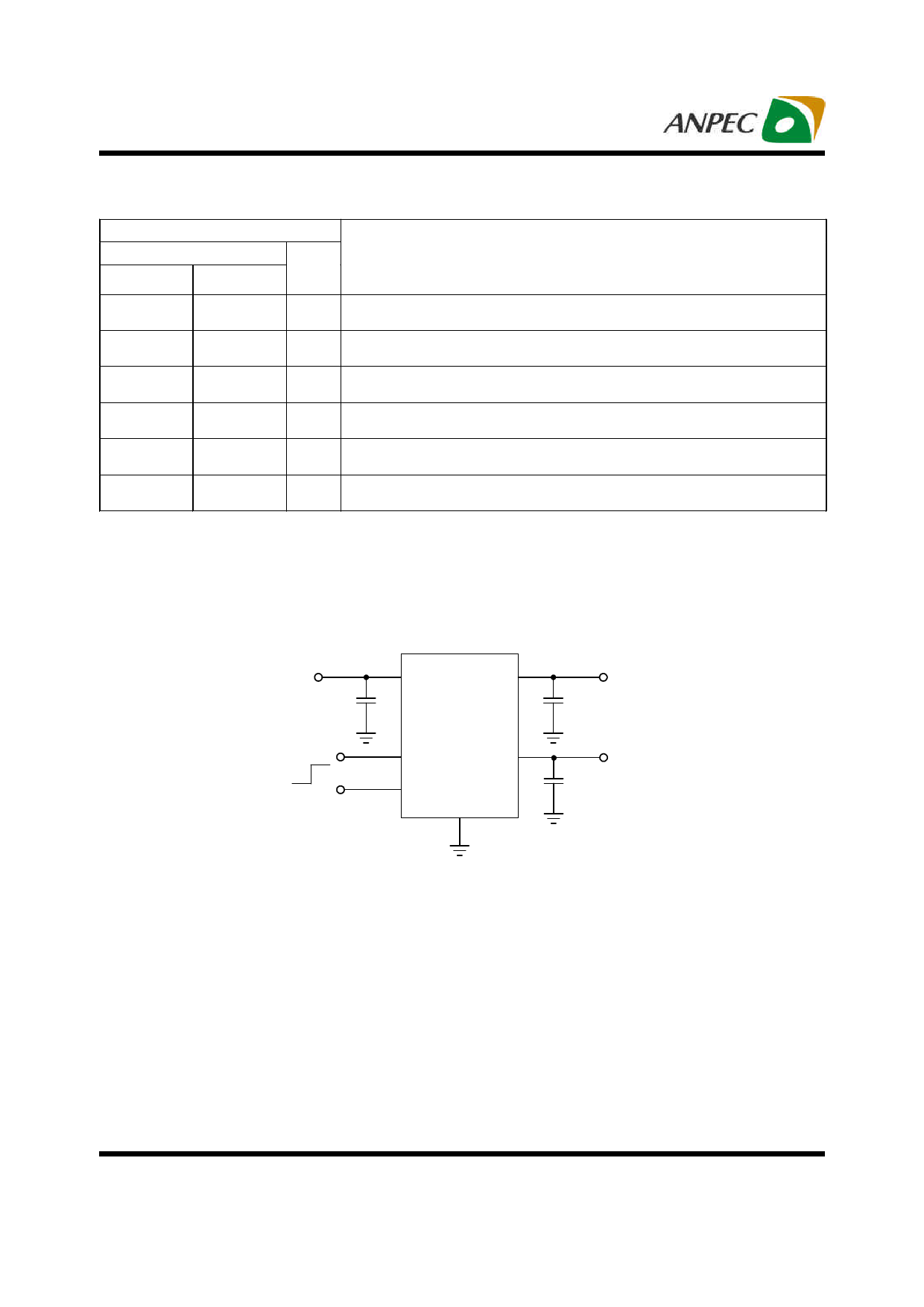
Typical Application Circuit
VIN
2.5V to 5.5V CIN
1µF
ON
OFF
VIN
VOUT1
APL5536
EN1
VOUT2
EN2
GND
COUT1
1µF
VOUT1
1.2V to 3.6V/300mA
COUT2
1µF
VOUT2
1.2V to 3.6V/300mA
Copyright © ANPEC Electronics Corp.
7
Rev. A.1 - Aug., 2010
www.anpec.com.tw
Share Link: 