APL5536JACI-TRG Просмотр технического описания (PDF) - Anpec Electronics
Номер в каталоге
Компоненты Описание
Список матч
APL5536JACI-TRG Datasheet PDF : 18 Pages
| |||
APL5536
Application Information
Input Capacitor
The APL5536 requires proper input capacitors to supply
surge current during stepping load transients to prevent
the input rail from dropping. Because the parasitic induc-
tor from the voltage sources or other bulk capacitors to
the VIN limit the slew rate of the surge current, place the
Input capacitors near VIN as close as possible. Input
capacitors should be larger than 1µF and a minimum
ceramic capacitor of 1µF is necessary.
Output Capacitor
The APL5536 needs a proper output capacitor to main-
tain circuit stability and improve transient response over-
temperature and current. In order to insure the circuit
stability, the proper output capacitor value should be larger
than 1µF. With X5R and X7R dielectrics, 1µF is sufficient
at all operating temperatures. Large output capacitor
value can reduce noise and improve load-transient re-
sponse and PSRR, Figure 1 shows the curves of allow-
able ESR range as the function of load current for various
output capacitor values.
Region of Stable COUT ESR vs. Output Current
10
APL5536-OC
VCIINN==4CVOUT=1µF/X7R
1
Unstable Range
where (T - T ) is the temperature difference between the
JA
junction and ambient air. θJA is the thermal resistance
between Junction and ambient air. Assuming the TA=25oC
and maximum TJ=160oC (typical thermal limit threshold),
the maximum power dissipation is calculated as:
PD(max) = (150-25)/220 = 0.568(W)
For normal operation, do not exceed the maximum junc-
tion temperature rating of T =125oC. The calculated power
J
dissipation should be less than:
PD = (125-25)/220 = 0.454(W)
The maximum power dissipation depends on operating
ambient temperature for fixed TJ(MAX) and thermal resis-
tance θJA. For SOT-23-6 package, the Figure 2 of derating
curves allows the designer to see the effect of rising
ambient temperature on the maximum power allowed.
The GND provides an electrical connection to the ground
and channels heat away. Connect the GND to the ground
by using a large pad or a ground plane.
0.6
Single Layer PCB
0.5
0.4
0.3
0.2
0.1
0.1
Stable Range
0.01
Simulation Verify
0.001 0
50
100
150 200 250
300
Output Current (mA)
Figure1. Stable COUT ESR Range
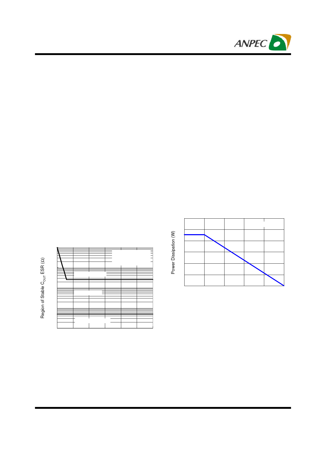
Operation Region and Power Dissipation
The APL5536 maximum power dissipation depends on
the thermal resistance and temperature difference be-
tween the die junction and ambient air. The SOT-23-6
package power dissipation PD across the device is:
PD = (TJ - TA) / θJA
0
0
25
50
75
100
125
Ambient Temperature (oC)
Figure 2. Derating Curves for SOT-23-6 Package
Layout Consideration
Figure 3 illustrates the layout. Below is a checklist for
your layout:
1. Please place the input capacitors close to the VIN.
2. Ceramic capacitors for load must be placed near the
load as close as possible.
3. To place APL5536 and output capacitors near the load
is good for performance.
4. Large current paths, the bold lines in Figure 3, must
have wide tracks.
Copyright © ANPEC Electronics Corp.
10
Rev. A.1 - Aug., 2010
www.anpec.com.tw
Share Link: 