CY7C1329_04 Просмотр технического описания (PDF) - Cypress Semiconductor
Номер в каталоге
Компоненты Описание
Список матч
CY7C1329_04 Datasheet PDF : 15 Pages
| |||
CY7C1329
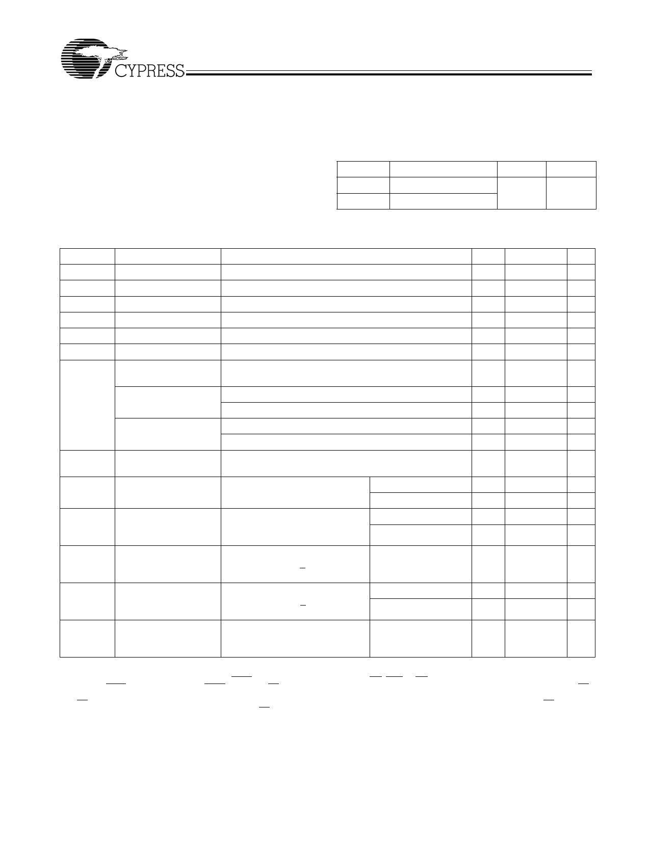
Maximum Ratings
(Above which the useful life may be impaired. For user guide-
lines, not tested.)
Storage Temperature ..................................... −65°C to +150°C
Ambient Temperature with
Power Applied.................................................. −55°C to +125°C
Supply Voltage on VDD Relative to GND.........−0.5V to +4.6V
DC Voltage Applied to Outputs
in High-Z State[7] .....................................−0.5V to VDDQ + 0.5V
DC Input Voltage[7]..................................−0.5V to VDDQ + 0.5V
Electrical Characteristics Over the Operating Range
Current into Outputs (LOW)......................................... 20 mA
Static Discharge Voltage........................................... >2001V
(per MIL-STD-883, Method 3015)
Latch-up Current..................................................... >200 mA
Operating Range
Range Ambient Temperature[8] VDD
VDDQ
Commercial
Industrial
0°C to +70°C
-40°C to +85°C
3.3V
3.3V
−5%/+10% −5%/+10%
Parameter
Description
Test Conditions
Min.
Max.
Unit
VDD
VDDQ
VOH
VOL
VIH
VIL
IX
Power Supply Voltage
I/O Supply Voltage
Output HIGH Voltage
Output LOW Voltage
Input HIGH Voltage
Input LOW Voltage[7]
Input Load Current
Except ZZ and MODE
3.3V −5%/+10%
3.3V −5%/+10%
VDD = Min., IOH = −4.0 mA
VDD = Min., IOL = 8.0 mA
GND ≤ VI ≤ VDDQ
3.135
3.6
V
3.135
3.6
V
2.4
V
0.4
V
2.0 VDDQ + 0.3V V
–0.3
0.8
V
−5
5
µA
Input Current of MODE Input = VSS
Input = VDDQ
Input Current of ZZ
Input = VSS
Input = VDDQ
IOZ
Output Leakage
GND ≤ VI ≤ VDDQ, Output Disabled
Current
–30
µA
5
µA
–5
µA
30
µA
−5
5
µA
IDD
VDD Operating Supply VDD = Max., IOUT = 0 mA,
7.5-ns cycle, 133 MHz
Current
f = fMAX = 1/tCYC
10-ns cycle, 100 MHz
325
mA
260
mA
ISB1
Automatic CS
Max. VDD, Device Deselected, 7.5-ns cycle, 133 MHz
Power-down
Current—TTL Inputs
VIN ≥ VIH or VIN ≤ VIL
f = fMAX = 1/tCYC
10-ns cycle, 100 MHz
ISB2
Automatic CS
Max. VDD, Device Deselected, All speeds
Power-down
VIN ≤ 0.3V or VIN > VDDQ – 0.3V,
Current—CMOS Inputs f = 0
60
mA
50
mA
5
mA
ISB3
Automatic CS
Max. VDD, Device Deselected, or 7.5-ns cycle, 133 MHz
Power-down
VIN ≤ 0.3V or VIN > VDDQ – 0.3V
Current—CMOS Inputs f = fMAX = 1/tCYC
10-ns cycle, 100 MHz
ISB4
Automatic CS
Max. VDD, Device Deselected,
Power-down
VIN ≥ VIH or VIN ≤ VIL, f = 0
Current—TTL Inputs
40
mA
30
mA
25
mA
Notes:
4. X = “Don't Care,” 1 = Logic HIGH, 0 = Logic LOW.
5. The SRAM always initiates a Read cycle when ADSP asserted, regardless of the state of GW, BWE, or BW[3:0]. Writes may occur only on subsequent clocks
after the ADSP or with the assertion of ADSC. As a result, OE must be driven HIGH prior to the start of the Write cycle to allow the outputs to three-state. OE
is a “don't care” for the remainder of the Write cycle.
6. OE is asynchronous and is not sampled with the clock rise. It is masked internally during Write cycles. During a Read cycle DQ = High-Z when OE is inactive
or when the device is deselected, and DQ = data when OE is active.
7. Minimum voltage equals –2.0V for pulse durations of less than 20 ns.
8. TA is the case temperature.
Document #: 38-05279 Rev. *B
Page 7 of 15
Share Link: 