CY7C1329_04 Просмотр технического описания (PDF) - Cypress Semiconductor
Номер в каталоге
Компоненты Описание
Список матч
CY7C1329_04 Datasheet PDF : 15 Pages
| |||
CY7C1329
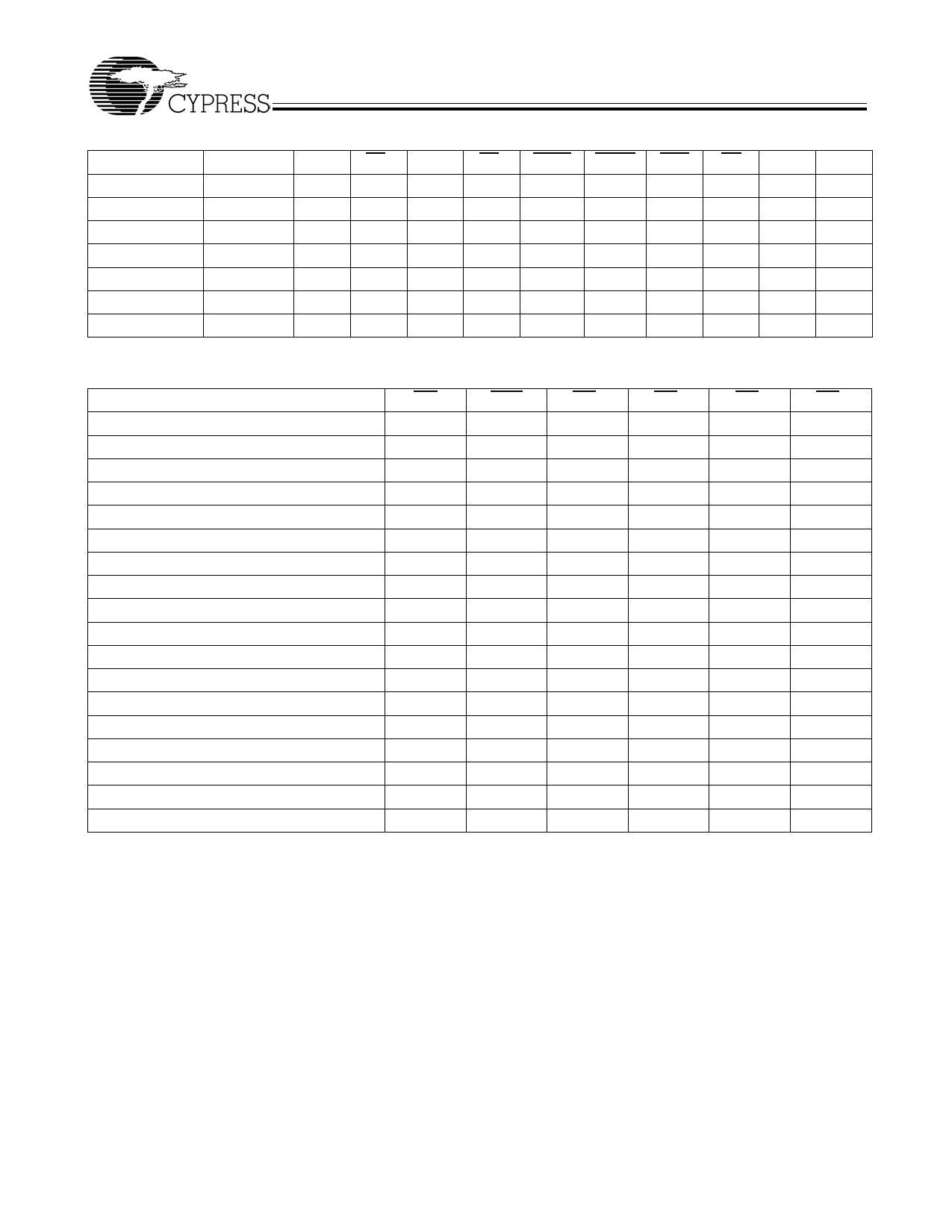
Cycle Descriptions (continued)[1,2,3]
Next Cycle Add. Used ZZ
Begin Write
Current
L
Begin Write
External
L
Continue Write Next
L
Continue Write Next
L
Suspend Write Current
L
Suspend Write Current
L
ZZ “sleep”
None
H
CE3 CE2 CE1 ADSP ADSC ADV OE
DQ Write
X
X
1
X
1
1
X Hi-Z Write
0
1
0
1
0
X
X Hi-Z Write
X
X
X
1
1
0
X Hi-Z Write
X
X
1
X
1
0
X Hi-Z Write
X
X
X
1
1
1
X Hi-Z Write
X
X
1
X
1
1
X Hi-Z Write
X
X
X
X
X
X
X Hi-Z X
Write Cycle Descriptions[4,5,6]
Function
Read
Read
Write Byte 0 – DQ[7:0]
Write Byte 1 – DQ[15:8]
Write Bytes 1, 0
Write Byte 2 – DQ[23:16]
Write Bytes 2, 0
Write Bytes 2, 1
Write Bytes 2, 1, 0
Write Byte 3 - DQ[31:24]
Write Bytes 3, 0
Write Bytes 3, 1
Write Bytes 3, 1, 0
Write Bytes 3, 2
Write Bytes 3, 2, 0
Write Bytes 3, 2, 1
Write All Bytes
Write All Bytes
GW
BWE
BW3
BW2
BW1
BW0
1
1
X
X
X
X
1
0
1
1
1
1
1
0
1
1
1
0
1
0
1
1
0
1
1
0
1
1
0
0
1
0
11
0
1
1
1
0
1
0
1
0
1
0
1
0
0
1
1
0
1
0
0
0
1
0
0
1
1
1
1
0
0
1
1
0
1
0
0
1
0
1
1
0
0
1
0
0
1
0
0
0
1
1
1
0
0
0
1
0
1
0
0
0
0
1
1
0
0
0
0
0
0
X
X
X
X
X
Document #: 38-05279 Rev. *B
Page 6 of 15
Share Link: 