LXE1686-0X Просмотр технического описания (PDF) - Microsemi Corporation
Номер в каталоге
Компоненты Описание
Список матч
LXE1686-0X Datasheet PDF : 15 Pages
| |||
LXE1686-0x
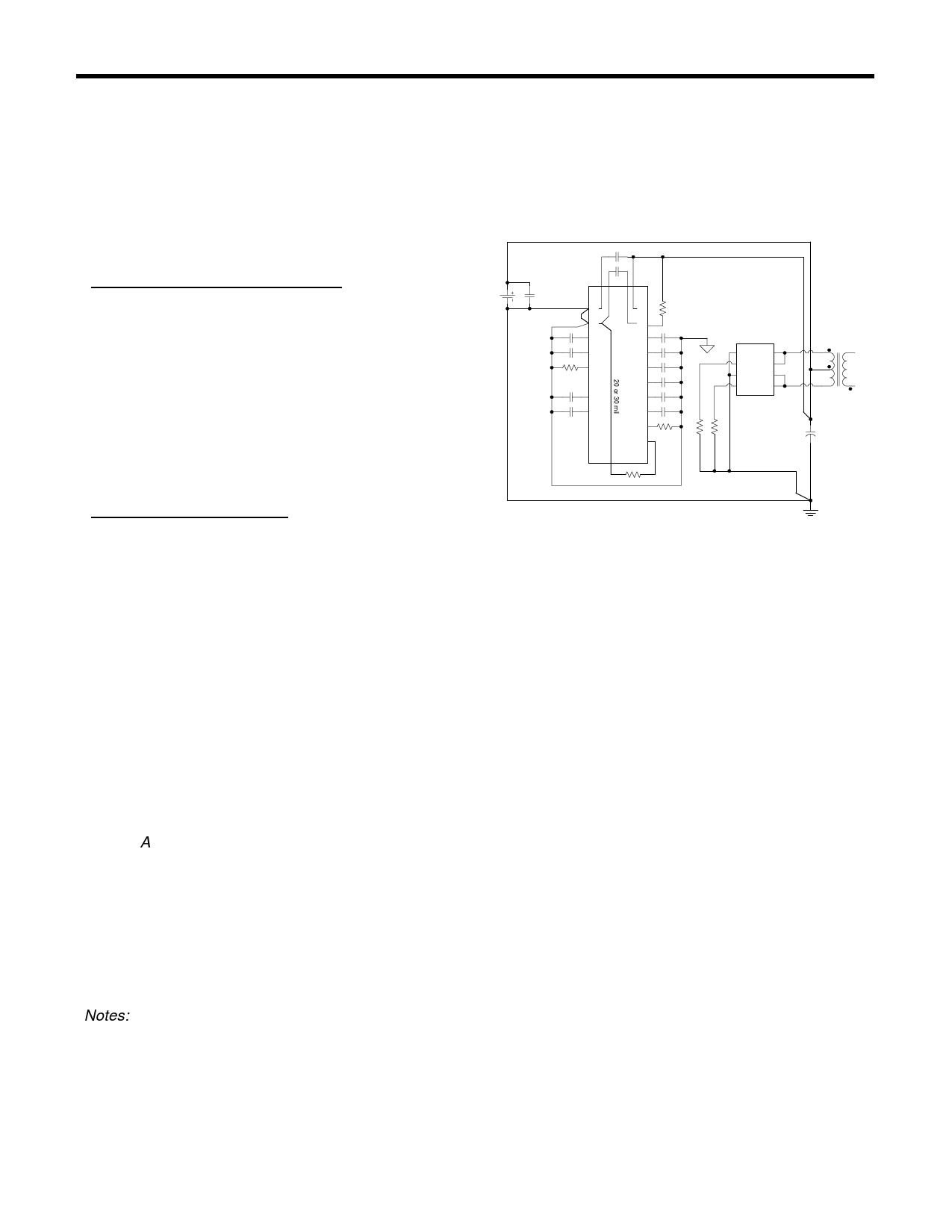
INVERTER EVALUATION BOARD
practice to provide a 1mm wide thru slot between
exposed solder contact points that are within 4mm of
one another (where high voltage potential exists) to
help disperse dust collection. No surface side traces
should route directly beneath the secondary portion of
the output transformer to avoid high voltage
breakdown.
HEAT TRANSFER AND NOISE RADIATION
It is acceptable and recommended to place large
copper areas beneath the output transformer primary
(but not beyond bobbin insulator) to help transfer heat
radiation. It is also recommended to enlarge the
copper areas connecting the FET drains and sources
for the same reason. It is not recommendable to place
any component circuitry (other than output transfer)
within 4mm of the output transformer secondary to
avoid the effects of high field noise radiation.
The following drawing will provide a reference for
critical component placement and power and ground
PCB trace routing as described in the first paragraph
of this section.
LX1686 Ideal PCB Power Trace Routing and
Critical Component Placement
40 mil trace width or more
100nF
1uF
100nF
1
2
20 or 30 mil
3
4
5
6
7
8
9
10
11
12
24
23
47 ohm
22
Analog GND
21
20
1
8
19
2
7
9945
3
6
18
4
5
17
16
Use copper area as
heatsink at fet sources
15
and drain as well as
tranformer primary
14
13
T1 LO
HIGH
100uF
PCB CAPACITOR FABRICATION
A small Pico-Farad value high voltage capacitor is
recommended for use on LX1686 inverter designs.
This capacitor accomplishes two critical functions:
• Reduce the open circuit self resonance of the
output transformer
• Configuration of a capacitive divider network to
sense and limit output transformer voltage potential
This capacitor (if used) can be either a vendor
component or it can be fabricated within your PCB
layout.
Follow the definitions and approximated formula
below to fabricate a PCB capacitor (accuracy of ±
20%).
A Copper area of each opposing PCB plate
surface (millimeter ²)
D Distance between opposing PCB plate
surfaces (millimeter)
C Desired capacitance (Farad)
ƒ Correlation factor (~ 20E12 millimeter/Farad)
Approximate formula: A = D × C × f
Notes:
'D' should not be less than 0.70mm and should dis-
count for copper thickness.
'A' should be round or have radius edges if rectangular
in shape.
Copyright © 2000
Rev 1.0c, 2000-08-31
40 mil trace width or more
Power GND
Page 13
Share Link: 