LXE1686-0X Просмотр технического описания (PDF) - Microsemi Corporation
Номер в каталоге
Компоненты Описание
Список матч
LXE1686-0X Datasheet PDF : 15 Pages
| |||
LXE1686-0x
INVERTER EVALUATION BOARD
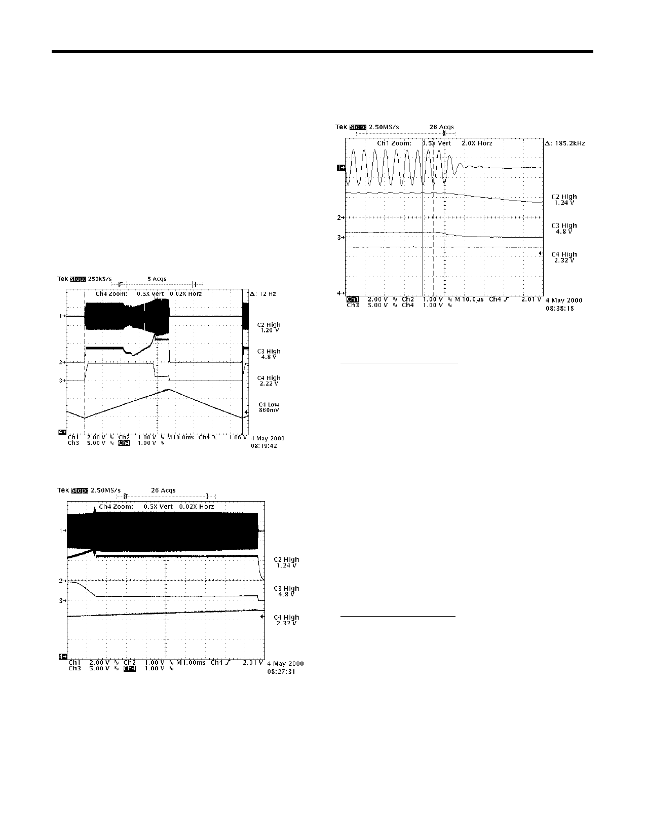
This next shot shows the strike method and open
circuit clamp. As the TRI_C ramp oscillator increases
the output frequency stays fixed until TRI_C reaches
the ramp change threshold of about 1.6V. Above this
threshold the output frequency and correspondingly
the output voltage increases until it hits the
overvoltage clamp. It remains at or near the clamp
voltage until the timeout period during the fall time of
TRI_C, after which it will attempt to strike the lamp
again.
Chan 1 TP4 (capacitive divider)
Chan 2 P14 (VSNS)
Chan 3 P15 (VCOMP)
Chan 4 P24 (TRI_C)
The shot below shows the peak frequency reached at
the peak of the TRI_C ramp 185KHz. This is in
contrast to the nominal run frequency of 65KHz.
Zoomed in shot of strike and overvoltage clamp.
5. PCB LAYOUT CONSIDERATIONS
POWER AND SIGNAL PLANE
Inverter PCB layout should be initially separated into
power and signal/analog level planes. Grounding of
these two planes should only be connected at one
common node, to avoid noise induction on sensitive
circuits. Ideally, this common node should be at the
main power filtering capacitor. Power level
components begin with the main power input
connector and end with the output transformer center-
tap. The FET sources conduct high current levels
back onto the power ground plane. The main filtering
capacitor should be located in close proximity to the
FET sources and output transformer center-tap. The
LX1686 VSS_P (pin2) and VDD_P (pin23) should
also be treated as power level nodes, as they
represent FET gate driver circuitry internal to the
LX1686. All other circuitry can be treated as
signal/analog level.
Copyright © 2000
Rev 1.0c, 2000-08-31
HIGH VOLTAGE CREEPAGE
Precautions with the high voltage secondary side of
the output transformer need to be observed. As this
inverter evaluation board is a single-ended concept,
only one pole of the output transformer will be at high
potential. This pole will connect to a ballast capacitor,
a capacitor divider then terminate to the high side
lamp output connector. These items will all be at high
potential and need at least 3mm of creepage
separation from all lower potential circuitry. Solder
masking of trace layout is required. It is a popular
Page 12
Share Link: 