RT5047 Просмотр технического описания (PDF) - Richtek Technology
Номер в каталоге
Компоненты Описание
Список матч
RT5047 Datasheet PDF : 16 Pages
| |||

Application Information
Boost Converter/Linear Regulator
The 5047 integrates a current-mode boost converter
and linear regulator. Use the SEL pin to control the
LNB voltage and the boost converter track is at least
greater 800mV than the LNB voltage. The boost
converter is high efficiency PWM architecture with
700kHz operation frequency. The linear regulator has
the capability to source current up to 550mA during
continuous operation. All the loop compensation,
current sensing, and slope compensation functions are
provided internally.
The RT5047 has current limiting on the boost converter
and the LNB output to protect the IC against short
circuits. The internal MOSFET will turn off when the LX
current is higher than 3A cycle-by-cycle. The LNB
output will turn off when the output current higher than
the 550mA and 45ms and turn-on after 1800ms
automatically.
Input Capacitor Selection
The input capacitor reduces voltage spikes from the
input supply and minimizes noise injection to the
converter. A 30F capacitance is sufficient for most
applications. Nevertheless, a higher or lower value may
be used depending on the noise level from the input
supply and the input current to the converter. Note that
the voltage rating of the input capacitor must be greater
than the maximum input voltage.
Inductor Selection
The inductance depends on the maximum input current.
As a general rule, the inductor ripple current range is
20% to 40% of the maximum input current. If 40% is
selected as an example, the inductor ripple current can
be calculated according to the following equations :
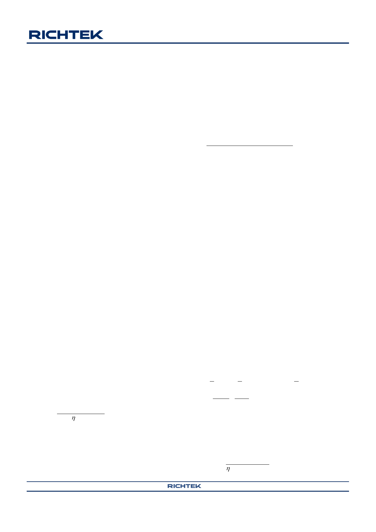
IIN(MAX)
=
VOUT IOUT(MAX)
VIN
IRIPPLE = 0.4 IIN(MAX)
where η is the efficiency of the converter, IIN(MAX) is
the maximum input current, and IRIPPLE is the
inductor ripple current. The input peak current can
then be obtained by adding the maximum input current
Copyright © 2015 Richtek Technology Corporation. All rights reserved.
DS5047-00 March 2015
RT5047
with half of the inductor ripple current as shown in the
following equation :
IPEAK = 1.2 x IIN(MAX)
note that the saturated current of the inductor must be
greater than IPEAK. The inductance can eventually be
determined according to the following equation :
L
η VIN 2 VOUT VIN
0.4 VOUT 2 IOUT(MAX)fOSC
where fOSC is the switching frequency. For better
system performance, a shielded inductor is preferred to
avoid EMI problems.
Boost Output Capacitor Selection
The RT5047 boost regulator is internally compensated
and relies on the inductor and output capacitor value
for overall loop stability. The output capacitor is in the
30F to 50F range with a low ESR, as strongly
recommended. The voltage rating on this capacitor
should be in the 25V to 35V range since it is connected
to the boost VOUT rail.
The output ripple voltage is an important index for
estimating chip performance. This portion consists of
two parts. One is the product of the inductor current
with the ESR of the output capacitor, while the other
part is formed by the charging and discharging process
of the output capacitor. As shown in Figure 1, VOUT1
can be evaluated based on the ideal energy
equalization. According to the definition of Q, the Q
value can be calculated as the following equation :
Q=
1
2
IIN
1
2
IL
IOUT
IIN
1
2
IL
IOUT
VIN
VOUT
1
fOSC
= COUT VOUT1
where fOSC is the switching frequency and IL is the
inductor ripple current. Bring COUT to the left side to
estimate the value of VOUT1 according to the following
equation :
VOUT1
=
D IOUT
COUT fOSC
is a registered trademark of Richtek Technology Corporation.
www.richtek.com
11