NCP1117DT285RKG(2014) Просмотр технического описания (PDF) - ON Semiconductor
Номер в каталоге
Компоненты Описание
Список матч
NCP1117DT285RKG
(Rev.:2014)
(Rev.:2014)
ON Semiconductor

NCP1117DT285RKG Datasheet PDF : 17 Pages
| |||
NCP1117, NCV1117
TYPICAL APPLICATIONS
Input
10
mF
3 NCP1117
XTXX
+
1
2 Output
+ 10
mF
110 W
Input 3 NCP1117 2 Output
XTA
10 +
+ 10
mF
1
mF
3 NCP1117 2
110 W
10 +
mF
XT285
1
+ 22 110 W
mF
4.75 V +
to
5.25 V
110 W
18 to 27
Lines
Figure 1. Fixed
Output Regulator
Figure 2. Adjustable
Output Regulator
Figure 3. Active SCSI Bus Terminator
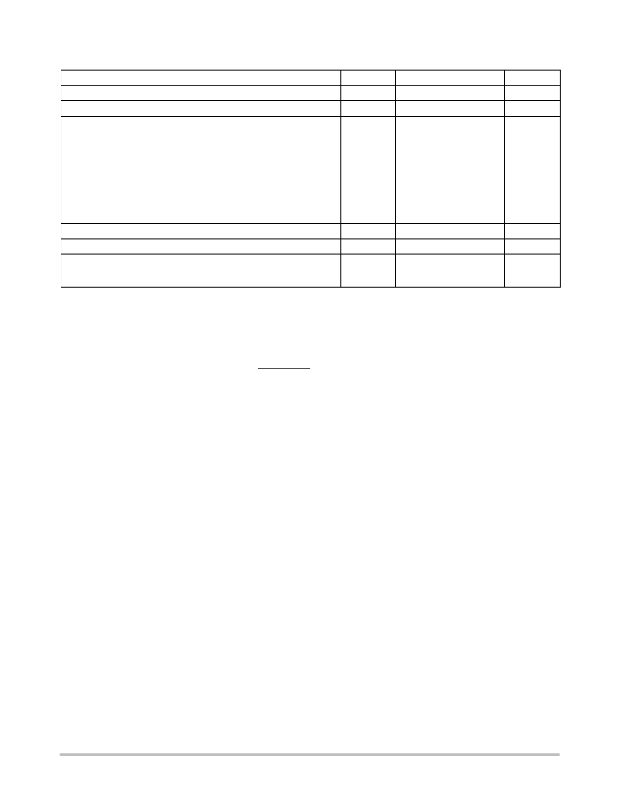
MAXIMUM RATINGS
Rating
Symbol
Value
Unit
Input Voltage (Note 1)
Output Short Circuit Duration (Notes 2 and 3)
Vin
20
V
−
Infinite
−
Power Dissipation and Thermal Characteristics
Case 318H (SOT−223)
Power Dissipation (Note 2)
Thermal Resistance, Junction−to−Ambient, Minimum Size Pad
Thermal Resistance, Junction−to−Case
Case 369A (DPAK)
Power Dissipation (Note 2)
Thermal Resistance, Junction−to−Ambient, Minimum Size Pad
Thermal Resistance, Junction−to−Case
Maximum Die Junction Temperature Range
Storage Temperature Range
Operating Ambient Temperature Range
NCP1117
NCV1117
PD
RqJA
RqJC
PD
RqJA
RqJC
TJ
Tstg
TA
Internally Limited
160
15
Internally Limited
67
6.0
−55 to 150
−65 to 150
0 to +125
−40 to +125
W
°C/W
°C/W
W
°C/W
°C/W
°C
°C
°C
Stresses exceeding those listed in the Maximum Ratings table may damage the device. If any of these limits are exceeded, device functionality
should not be assumed, damage may occur and reliability may be affected.
1. This device series contains ESD protection and exceeds the following tests:
Human Body Model (HBM), Class 2, 2000 V
Machine Model (MM), Class B, 200 V
Charge Device Model (CDM), Class IV, 2000 V.
2. Internal thermal shutdown protection limits the die temperature to approximately 175°C. Proper heatsinking is required to prevent activation.
The
maximum
package
power
dissipation
is:
PD
+
TJ(max) *
RqJA
TA
3. The regulator output current must not exceed 1.0 A with Vin greater than 12 V.
http://onsemi.com
2
Share Link: