74ABT543A Просмотр технического описания (PDF) - NXP Semiconductors.
Номер в каталоге
Компоненты Описание
Список матч
74ABT543A Datasheet PDF : 17 Pages
| |||
NXP Semiconductors
74ABT543A
Octal latched transceiver with dual enable; 3-state
VI
An, Bn
GND
VI
LEAB, LEBA,
EAB, EBA
GND
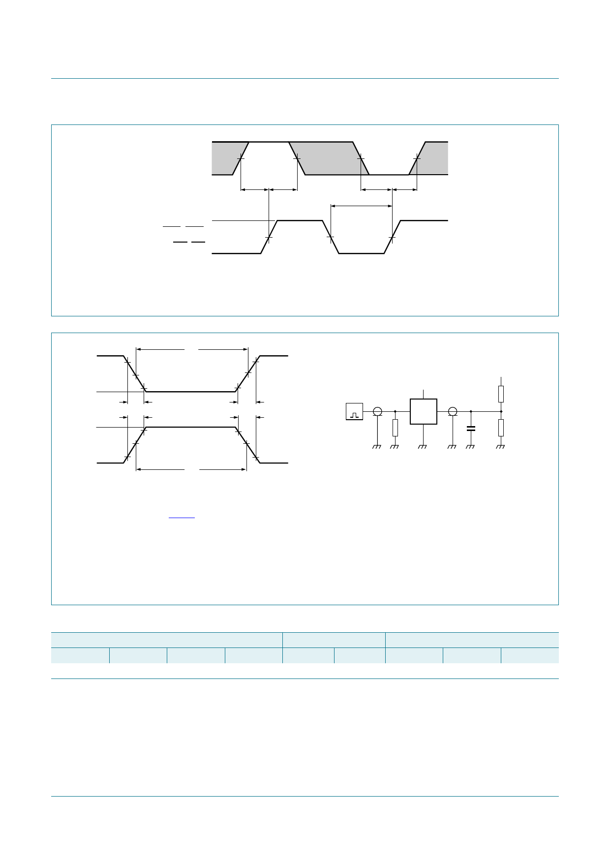
VM
VM
tsu(H) th(H)
VM
VM
VM
tsu(L)
tWL
th(L)
VM
001aae905
Fig 9.
VM = 1.5 V.
The shaded areas indicate when the input is permitted to change for predictable output performance.
Data set-up and hold times and latch enable pulse width
VI
negative
pulse
0V
VI
positive
pulse
0V
90 %
10 %
VM
10 %
tf
tr
90 %
VM
tW
90 %
VM
10 %
tr
tf
90 %
VM
10 %
tW
001aai298
VI
G
VCC
VO
DUT
RT
a. Input pulse definition
b. Test circuit
Test data is given in Table 8.
Test circuit definitions:
RL = Load resistance.
CL = Load capacitance including jig and probe capacitance.
RT = Termination resistance should be equal to output impedance Zo of the pulse generator.
VEXT = Test voltage for switching times.
Fig 10. Load circuitry for switching times
VEXT
RL
CL
RL
mna616
Table 8.
Input
VI
3.0 V
Test data
fI
1 MHz
tW
500 ns
tr, tf
2.5 ns
Load
CL
50 pF
RL
500
VEXT
tPHL, tPLH
open
tPZH, tPHZ
open
tPZL, tPLZ
7.0 V
74ABT543A
Product data sheet
All information provided in this document is subject to legal disclaimers.
Rev. 5 — 3 November 2011
© NXP B.V. 2011. All rights reserved.
9 of 16
Share Link: 