HEF4520BP,652 Просмотр технического описания (PDF) - NXP Semiconductors.
Номер в каталоге
Компоненты Описание
Список матч
HEF4520BP,652 Datasheet PDF : 14 Pages
| |||
NXP Semiconductors
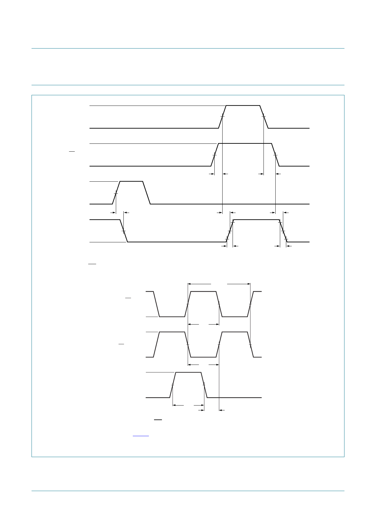
11. Waveforms
HEF4520B
Dual binary counter
VI
nCP0 input
VM
0V
VI
nCP1 input
0V
VI
nMR input
0V
VOH
nQn output
VOL
0V
VM
tPHL
VM
tsu
tPLH
90 %
10 %
tt
a. nCP0 and nCP1 set-up times, propagation delays and output transition times
VM
tsu
tPHL
tt
001aae702
VI
nCP1 input
(nCP0 = LOW)
0V
VI
nCP0 input
(nCP1 = HIGH)
0V
VI
1/fmax
VM
tW
VM
tW
nMR input
VM
0V
tW
trec
001aae701
b. nMR recovery time, minimum nCP0, nCP1, and nMR pulse widths and maximum frequency
Fig 5.
Measurement points are given in Table 9.
The logic levels VOH and VOL are typical output voltage levels that occur with the output load.
Waveforms showing measurements for switching times
HEF4520B
Product data sheet
All information provided in this document is subject to legal disclaimers.
Rev. 6 — 18 November 2011
© NXP B.V. 2011. All rights reserved.
7 of 14
Share Link: 