W6662CF Просмотр технического описания (PDF) - Winbond
Номер в каталоге
Компоненты Описание
Список матч
W6662CF Datasheet PDF : 19 Pages
| |||
Preliminary W6662CF
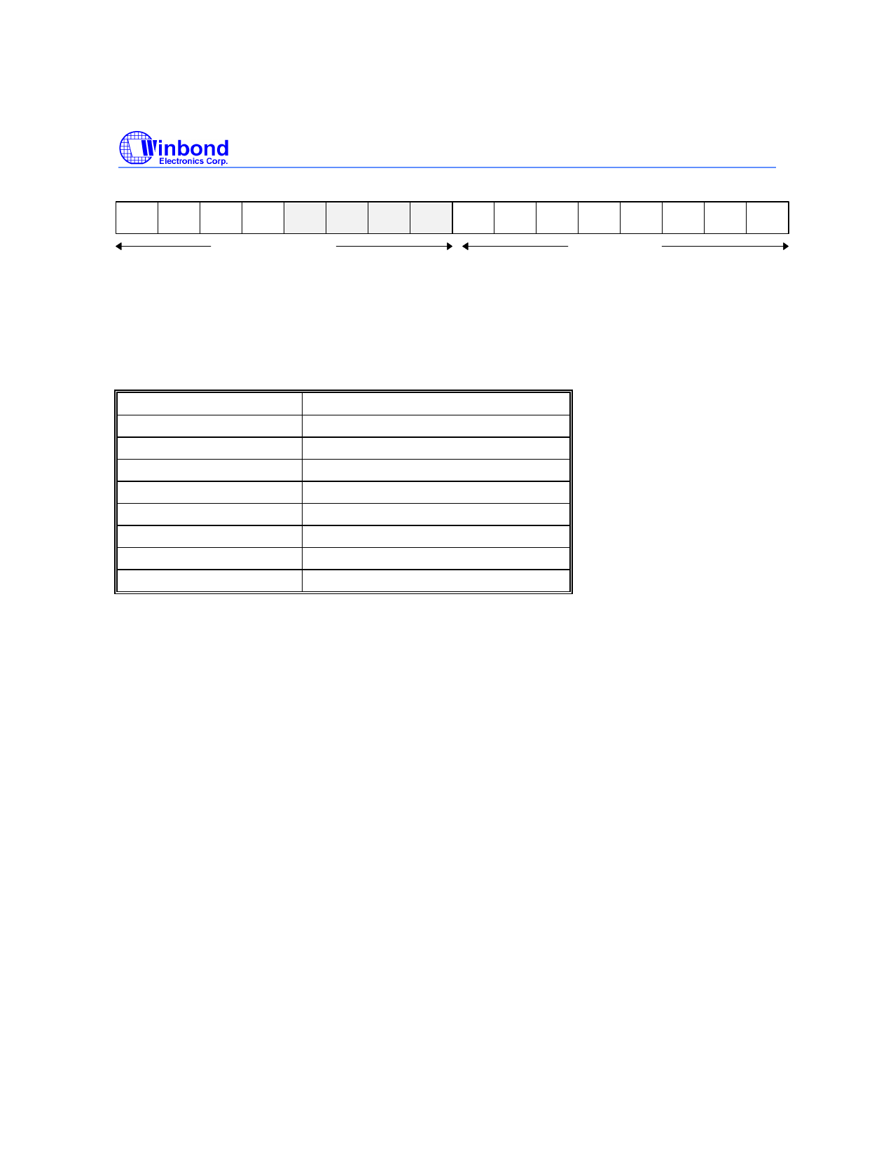
R/W A0 A1 A2 -- -- -- -- D0 D1 D2 D3 D4 D5 D6 D7
Address phase
Data phase
R/W is read (high) or write (low) command to access the register.
A0, A1 and A2 is the address select bits of the register.
D0 throuth D7 is the data bit of the register, D7 is MSB and D0 is LSB.
The address of the registers is:
A2
A1
A0
REGISTER
0
0
0 Configuration Register
0
0
1 Red PGA Register
0
1
0 Green PGA Register
0
1
1 Blue PGA Register
1
0
0 Red Offset Register
1
0
1 Green Offset Register
1
1
0 Blue Offset Register
1
1
1 Reserved
Configuration Register
The bit definition of configuration register is:
A. Configuration mode (wake up and configuration)
bit 0 = 0: 1.5V input span.
1: 3.0V input span.
bit 1 = 0: S&H mode.
1: CDS mode.
bit [3:2] = 0 0: Red channel input only.
0 1: Green channel input only.
1 0: Blue channel input only.
1 1: Three channels input and selected by SEL1 and SEL0 signals.
bit 4 = Reserved (must set to 0).
bit 5 = 0: PAOUT and PAOUTN enable.
1: PAOUT and PAOUTN disable.
bit 6 = Reserved (must set to 0).
bit 7 = 0.
-8-
Share Link: 