W6662CF Просмотр технического описания (PDF) - Winbond
Номер в каталоге
Компоненты Описание
Список матч
W6662CF Datasheet PDF : 19 Pages
| |||
Preliminary W6662CF
PGA Gain Adjustment
"PGA" stands for "programmable gain amplifier", it can provide analog gain for "not enough level for
A/D converter" input signals. The gain value is converted from PGA_code of gain register and is
selected by channel select SEL1 and SEL0. The gain formula is:
analog gain = 1 +
PGA_code
12
PGA_code = 0−63 and the gain = 1−6.25.
Offset Adjustment
The analog signal level can be shifted by offset level and to get maximum linear region. The offset
level is converted from offset value by internal D/A converter and the offset value is selected by
channel select SEL1 and SEL0.
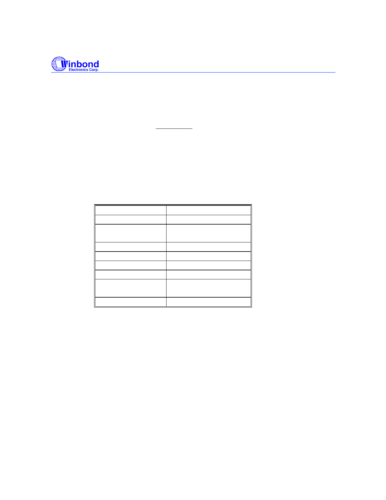
The mapping between offset register code and offset value is as follows:
OFFSET REGISTER
1111 1111 (LSB)
:
:
1000 0001
1000 0000
0000 0000
0000 0001
:
:
0111 1111
OFFSET VALUE
+200 mV
:
:
+1.6 mV
0.0 mV
0.0 mV
-1.6 mV
:
:
-200 mV
6.5 Analog Monitor
The analog differential signal of PAOUT and PAOUTN is used to monitor the output waveform after
gain and offset adjustment process. The CCD or CIS pixel rate must operate below or equal 1MHz
and at most one probe loading on the PAOUT and PAOUTN to get a correct voltage output. In normal
operation, the PAOUT and PAOUTN must be turned off by writting a specified bit on the configuration
register to avoid the interference of noise and extra capacitance loading.
6.6 Internal Registers
The registers in the W6662 is configuration register, three channel offset registers and three channel
gain registers, these registers are addressed by A2, A1 and A0. The registers can be read or modified
through 3-wired or four-wired serial interface. During address phase, if SDO/SMS pin is low, three-
wired is selected, the three-wired interface are SEN, SCLK and SDIO signals, if SDO/SMS pin is
high, four-wired interface is selected, the four-wired interface are SEN, SCLK SDI and SDO signals.
Figure 6-4 shows the setting of the serial interface. For three-wired interface setting, the SDO/SMS
pin must connected to VSS. For four-wired interface, it only need to connect a pull high resistor on the
SDO/SMS pin. The signal format on the serial interface is listed as follows:
Publication Release Date: December 1998
-7-
Revision A1
Share Link: 