STK11C68 Просмотр технического описания (PDF) - Cypress Semiconductor
Номер в каталоге
Компоненты Описание
Список матч
STK11C68 Datasheet PDF : 16 Pages
| |||
STK11C68
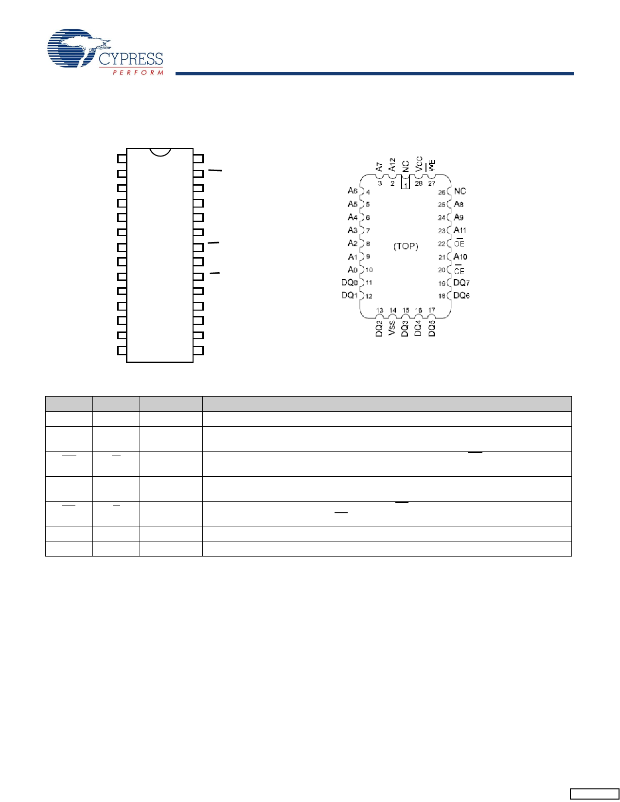
Pin Configurations
Figure 1. Pin Diagram - 28-Pin SOIC/DIP and 28-Pin LLC
1&
$
$
$
$
$
$
$
$
$
'4
'4
'4
966
723
9&&
:(
1&
$
$
$
2(
$
&(
'4
'4
'4
'4
'4
Pin Definitions
Pin Name Alt
IO Type
Description
A0–A12
DQ0-DQ7
Input
Input or
Output
Address Inputs. Used to select one of the 8,192 bytes of the nvSRAM.
Bidirectional Data IO Lines. Used as input or output lines depending on operation.
WE
W
Input
Write Enable Input, Active LOW. When the chip is enabled and WE is LOW, data on the
IO pins is written to the specific address location.
CE
E
Input
Chip Enable Input, Active LOW. When LOW, selects the chip. When HIGH, deselects the
chip.
OE
G
Input
Output Enable, Active LOW. The active LOW OE input enables the data output buffers
during read cycles. Deasserting OE HIGH causes the IO pins to tri-state.
VSS
Ground Ground for the Device. The device is connected to ground of the system.
VCC
Power Supply Power Supply Inputs to the Device.
Document Number: 001-50638 Rev. **
Page 2 of 16
[+] Feedback
Share Link: 