MB90440G Просмотр технического описания (PDF) - Fujitsu
Номер в каталоге
Компоненты Описание
Список матч
MB90440G Datasheet PDF : 61 Pages
| |||
MB90440G Series
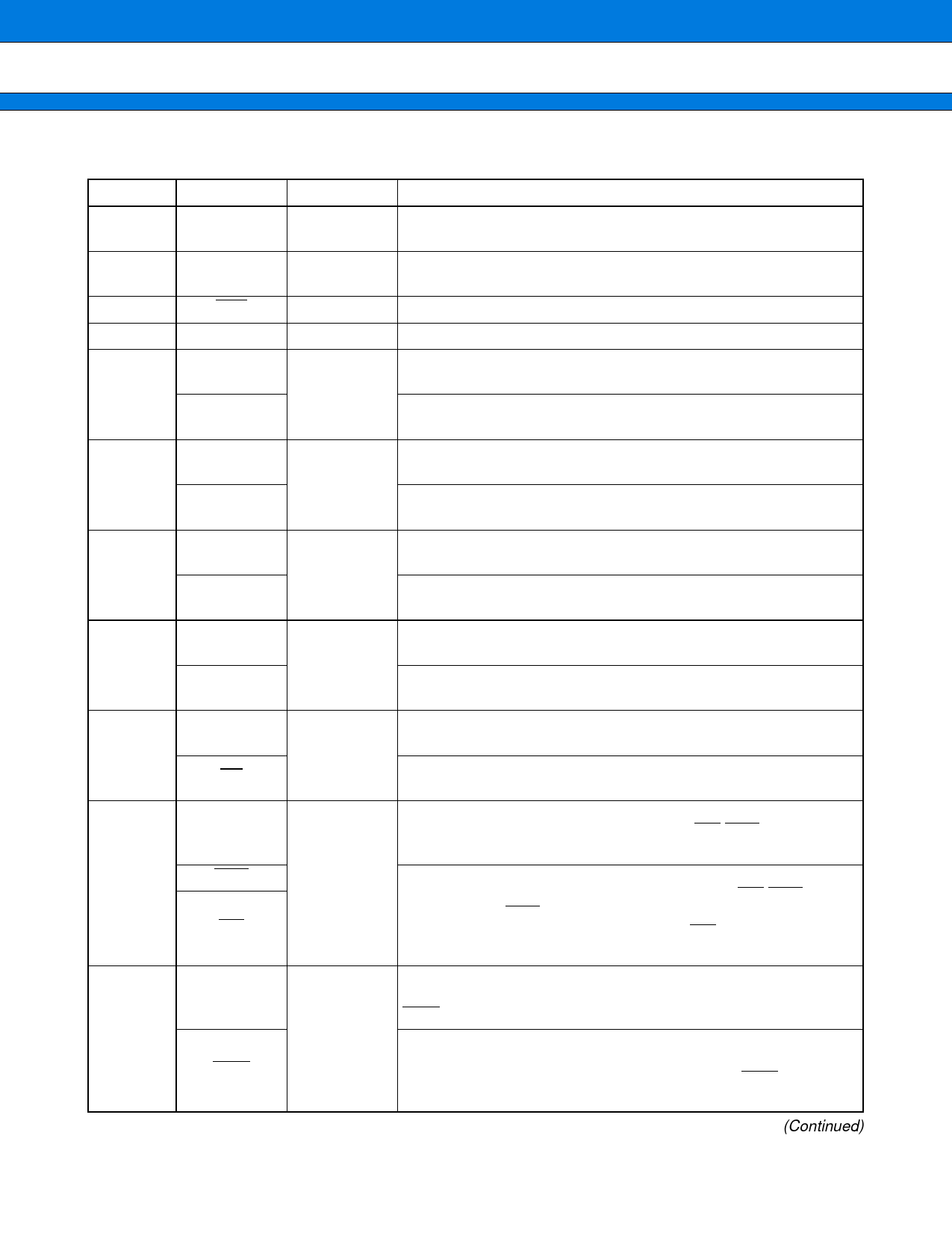
s PIN DESCRIPTION
Pin No. Pin name Circuit type
Function
82
83
X0
X1
A
(Oscillation)
High speed oscillator input pins
80
79
X0A
X1A
A
(Oscillation)
Low speed oscillator input pins
77
RST
B
External reset request input
52
N.C.
not connected
P00 to P07
General I/O port with programmable pullup. This function is en-
abled in the single-chip mode.
85 to 92
H
AD00 to AD07
I/O pins for 8 lower bits of the external address/data bus. This func-
tion is enabled when the external bus is enabled.
P10 to P17
General I/O port with programmable pullup. This function is en-
abled in the single-chip mode.
93 to 100
H
AD08 to AD15
I/O pins for 8 higher bits of the external address/data bus. This func-
tion is enabled when the external bus is enabled.
1 to 8
P20 to P27
A16 to A23
General I/O port with programmable pullup. This function is en-
abled in the single-chip mode.
H
I/O pins of 8 bits for A16 to A23 ot the external address bus. This
function is enabled when the external bus is enabled.
P30
9
ALE
General I/O port with programmable pullup. This function is en-
abled in the single-chip mode.
H
Address latch enable output pin. This function is enabled when the
external bus is enabled.
P31
10
RD
General I/O port with programmable pullup. This function is en-
abled in the single-chip mode.
H
Read strobe output pin for the data bus. This function is enabled
when the external bus is enabled.
General I/O port with programmable pullup. This function is en-
P32
abled in the single-chip mode or when the WR/WRL pin output is
disabled.
12
WRL
WR
H
Write strobe output pin for the data bus. This function is enabled
when the external bus is in enable mode and the WR/WRL pin out-
put is enabled. WRL is used as a write-strobe output pin for 8 lower
bits of the data bus in 16-bit access while WR is used as a write-
strobe output pin for 8 bits of the data bus in 8-bit access.
P33
13
WRH
General I/O port with programmable pullup. This function is en-
abled in the single-chip mode or external bus 8-bit mode or when
WRH pin output is disabled.
H
Write strobe output pin for the 8 higher bits of the data bus. This
function is enabled when the external bus is enabled, when the ex-
ternal bus 16-bit mode is selected, and when the WRH output pin
is enabled.
(Continued)
7
Share Link: 