M65762FP Просмотр технического описания (PDF) - Renesas Electronics
Номер в каталоге
Компоненты Описание
Список матч
M65762FP Datasheet PDF : 35 Pages
| |||
M65762FP
2. Description on Register
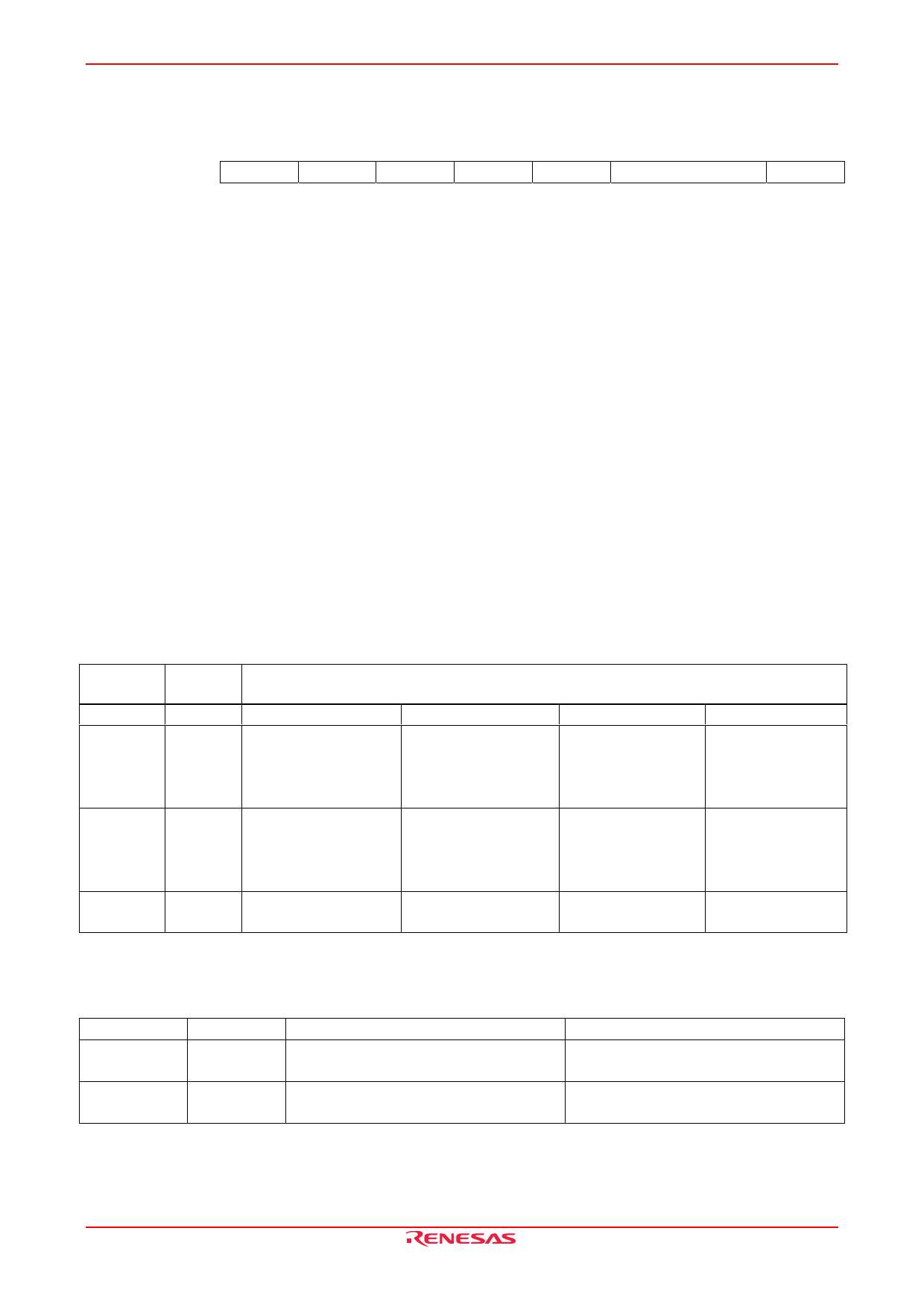
(1) System setting register (W/R)
(Address: 0)
d7(MSB)
SYS_REG:
PB
PI
BX
BS
DS
d0 (LSB)
CB
HR
d0 (HR):
d1 to 2 (CB):
d3 (DS):
d4 (BS):
d5 (BX):
d6 (PI):
d7 (PB):
H/W reset (0: Active status, 1: Reset status)
To reset H/W, set this bit to 1 then to 0. The entire LSI including register group and line memory is
initialized by writing in this reset. However, context table RAM is not initialized.
Selects the bit width of code data bus
(d2 = 0, d1 = 0: 8-bit bus (CD0 to 7), d2 = 0, d1 = 1: 16-bit bus (CD0 to 15), d2 = 1, d1 = 0: 32-bit bus
(CD0 to 31))
Notes: 1. Prohibition of setting for d2 = 1, d1 = 1
2. For encoding in 16-/32-bit bus, the last encoding data is output followed by bit byte of "00"
(3 bytes maximum) for word alignment of encoding data at the end.
Selects data bit swap of image data bus (0: MSB first, 1: LSB first) → see table 3.
Selection of data bit swap of code data bus (0: MSB first, 1: LSB first) → see table 2.
Selection of data byte swap of code data bus
(0: low order byte first, 1: high order byte first) → see table 2.
Note: BX is effective only when the host bus selects 16-bit/32-bit bus.
Selection of image data input/output I/F (0: serial I/F, 1: parallel I/F)
Selection of bit width of image data bus
(0: 32-bit bus (PD0 to 31), 1: 16-bit bus (PD0 to 15) → see table 3.
Note: PB and DS are effective only when PI = 1.
Table 2 Line Up of Coded Data/Image Data in Code Data Bus
Bus Width Swap
(CB)
(BX, BS)
Order of Data in Code Data Bus (CD)
d2 d1 d5 d4 CD31 • • • CD24 CD23 • • • CD16 CD15 • • • CD8 CD7 • • • CD0
1 0 0 0 b24 • • • b31 b16 • • • b23 b8 • • • b15 b0 • • • b7
(32 bits) 0 1 b31 • • • b24 b23 • • • b16 b15 • • • b8 b7 • • • b0
1 0 b0 • • • b7
b8 • • • b15 b16 • • • b23 b24 • • • b31
1 1 b7 • • • b0
b15 • • • b8 b23 • • • b16 b31 • • • b24
0 1 00
—
—
b8 • • • b15 b0 • • • b7
(16 bits) 0 1
—
—
b15 • • • b8 b7 • • • b0
10
—
—
b0 • • • b7 b8 • • • b15
11
—
—
b7 • • • b0 b15 • • • b8
0 0 —0
—
—
—
b0 • • • b7
(8 bits) — 1
—
—
—
b7 • • • b0
Note: b0 is image data, given in time series, on the left side of the first encoding data/screen. b31 is image data, given
in time series, on the right side of the last encoding data/screen.
Table 3 Order of Image Data on Image Data Parallel Bus
Bit Width
Swap
PD31
•••••
PD16
PD15
•••••
PD0
PB = 0
DS = 0
p0
•••••
p15
p16
•••••
p31
DS = 1
p31
•••••
p16
p15
•••••
p0
PB = 1
DS = 0
—
p0
•••••
p15
DS = 1
—
p15
•••••
p0
Note: p0 is image data on the left side of the screen. p31 is image data on the right side of the screen.
REJ03F0235-0200 Rev.2.00 Sep 14, 2007
Page 10 of 34
Share Link: 