IR5001 Просмотр технического описания (PDF) - International Rectifier
Номер в каталоге
Компоненты Описание
Список матч
IR5001 Datasheet PDF : 13 Pages
| |||
IR5001
APPLICATION INFORMATION
The IR5001 is designed for multiple active ORing
and reverse polarity protection applications with
minimal number of external components. Examples
of typical circuit connections are shown below.
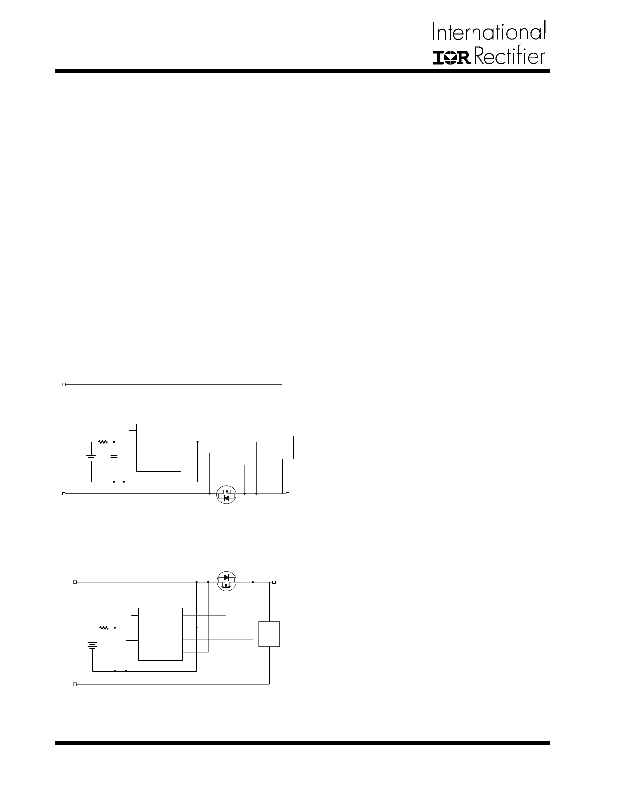
Negative Rail ORing/Reverse Polarity Protection
A typical connection of the IR5001 in negative
rail Active ORing or reverse polarity protection is
shown in Fig. 17. In this example, IR5001 is biased
directly from the positive rail. However, any of the
biasing schemes shown in Fig. 16 can be used.
For input ORing in carrier-class communications
boards, one IR5001 is used per feed. This is shown
in Fig.1. An evaluation kit is available for typical
system boards, with input voltages of negative 36V
to negative 75V, and for power levels from 30W to
about 300W. The p/n for the evaluation kit is
IRDC5001-LS48V. This evaluation kit contains
detailed design considerations and in-circuit
performance data for the IR5001.
Vin +
Rbias
+
Vbias
IR5001
Vline
OUT
Vcc
Gnd
FETch
INN
FETst
INP
Load
Vin -
Redundant Vin -
Figure. 17 Connection of INN, INP, and Gnd for negative
rail Active ORing or reverse polarity protection.
Vout +
Redundant Vout +
Rbias
+
Vbias
Vout -
IR5001
Vline
OUT
Vcc
Gnd
FETch INN
FETst
INP
Load
Figure. 18. Connection of INN,INP, and Gnd when the
MOSFET is placed in the path of positive rail.
Positive Rail ORing / Ground ORing in
Communications Boards
An example of a typical connection in positive
rail ORing is shown in Fig. 18. Typical applications
are inside redundant AC-DC and DC-DC power
supplies, or on-board ORing. For positive rail ORing,
an additional Vbias voltage above the positive rail is
needed to bias the IR5001.
An evaluation kit for high-current 12V positive
rail ORing is available under p/n IRAC5001-
HS100A, demonstrating performance of the IR5001
at 100A output current.
Considerations for the Selection of the Active
ORing N-Channel MOSFET
Active ORing FET losses are all conduction
losses, and depend on the source-drain current and
RDS(on) of the FET. The conduction loss could be
virtually eliminated if a FET with very low RDS(on)
was used. However, using arbitrarily low RDS(on) is
not desirable for three reasons:
1. Turn off propagation delay. Higher RDS(on) will
provide more voltage information to the internal
comparator faster, and will result in faster FET
turn off protection in case of short-circuit of the
source (less voltage disturbance on the
redundant bus.
2. Undetected reverse (drain to source) current
flow. With the asymmetrical offset voltage, some
small current can flow from the drain to source
of the ORing FET and be undetected by the
IR5001. The amount of undetected drain-source
current depends on the RDS(on) of the selected
MOSFET and its RDS(on). To keep the reverse
(drain-source) current below 5 – 10% of the
nominal source-drain state, the RDS(on) of the
selected FET should produce 50mV to 100mV of
the voltage drop during nominal operation.
3. Cost. With properly selected RDS(on), Active
ORing using IR5001 can be very cost
competitive with traditional ORing while
providing huge power loss reduction. For
example, a FET with 20mOhm RDS(on) results in
60mV voltage drop at 3A; associated power
savings compared to the traditional diode ORing
(assuming typical 0.6V forward voltage drop) is
ten fold(0.18W vs. 1.8W)! Now assume that
FET RDS(on) was 10mOhm. The power loss
would be reduced by additional 90mW, which is
negligible compared to the power loss reduction
already achieved with 20mOhm FET. But to get
this negligible saving, the cost of the Active
ORing FET would increase significantly.
10
www.irf.com
Share Link: 