ML4813CP Просмотр технического описания (PDF) - Micro Linear Corporation
Номер в каталоге
Компоненты Описание
Список матч
ML4813CP Datasheet PDF : 15 Pages
| |||
APPLICATIONS (Continued)
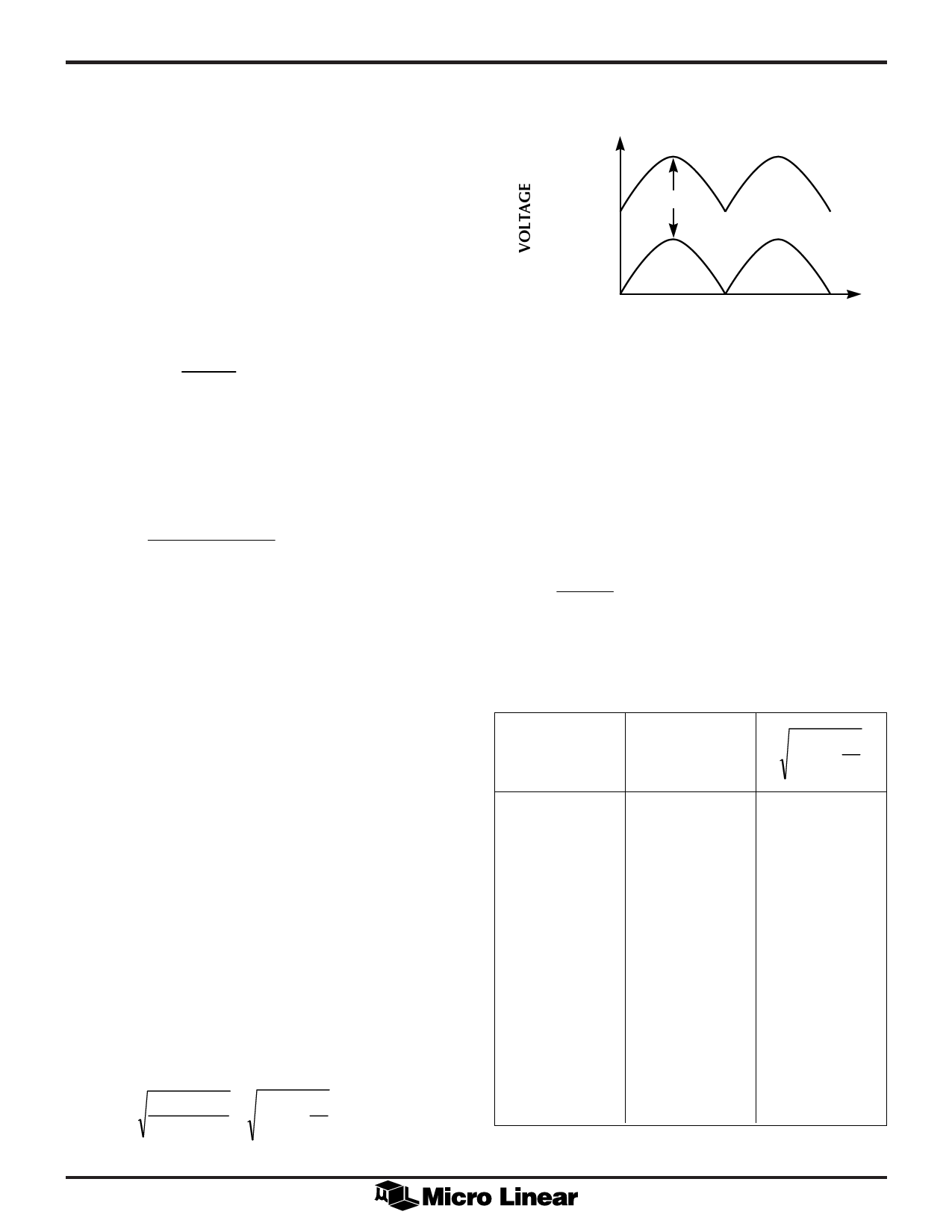
The output voltage "rides" on the input voltage when the
(+) output is measured with respect to PWR GND as
shown in Figure 10.
The extra op amp provided in the ML4813 can be used to
sense the output voltage for regulation and overvoltage
conditions. This op amp is connected as a difference
amplifier with its output referenced to PWR GND.
Resistors RH1, RH2, RL1, RL2 are used to scale down the
voltage.
Normally, RH1 = RH2 = RH and RL1 = RL2 = RL. The
voltage designated as VS in Figure 7 is given by:
VS
=
VOUT
RL
RH + RL
(16)
The output capacitance should be calculated such that it
has the required output ripple at the worst case operating
point. In addition, the ESR should be sufficiently low to
prevent excessive dissipation due to RMS currents. The
first criterion can be met by choosing the value of the
output capacitor based on the following:
COUT
2pfL
PIN
DVR
VOUT
(17)
Where:
COUT = Total output capacitance
PIN = Total input power
DVR = Peak output capacitor ripple voltage
fL = Line frequency times 2 (120 for 60Hz line)
The second criterion for the selection of the output
capacitor can be satisfied by choosing a component with
adequately low ESR value that can safely bypass the RMS
currents.
OUTPUT DIODE
The output diode can be a "fast" or ultrafast' type
depending on the operating frequency. Reverse recovery
losses are low since under normal operating conditions,
the regulator operates in discontinuous current mode. The
diode should be rated to handle the maximum output
current. The resulting power dissipation will be the
forward drop of the diode times the output current.
POWER SWITCH
If a power MOSFET is used, it should be sized for the
required efficiency. Lower RDS(ON) devices will yield
lower losses, but if they are operated at high frequencies
(100kHz), higher charge dumping losses will be
experienced. The RMS current value through the power
FET and the sensing resistor is:
Ê IRMS =
L IP 3 fL
4.24 VRMS
r sin2 kp
k=1
r
(15)
ML4813
200V
VOUT
VOUT+
PWR GND
TIME
VOUT-
Figure 10. Output Voltage with Respect to PWR GND
Where:
IRMS = Total RMS current through the power MOSFET
fL = Line frequency times 2 (120 for 60Hz line)
r = fSWITCH/fL
Table 1 is provided to assist in calculating (18). When the
power switch is a bipolar transistor (constant VCE drop),
then the power dissipation produced can be calculated
by:
PD
=
0.9 PIN
VRMS
VCE
(19)
Where:
PD = Power dissipation in the transistor
VRMS = RMS value of the minimum input voltage
VCE = Forward drop of the power transistor
fSWITCH
(kHz)
r
Êr sin2 kp
k=1
r
20
167
9.1
30
250
11.2
40
333
12.9
50
417
14.4
60
500
25.8
70
583
17.1
80
667
18.3
90
750
19.4
100
833
20.4
110
917
21.4
120
1000
22.4
130
1083
23.3
140
1167
24.2
150
1250
25.0
160
1333
25.7
170
1417
26.5
180
1500
27.3
190
1583
28.0
200
1667
28.9
Table 1. Constants for Calculating IRMS (Equation 18)
11
Share Link: 