CS8129(2008) Просмотр технического описания (PDF) - ON Semiconductor
Номер в каталоге
Компоненты Описание
Список матч
CS8129
(Rev.:2008)
(Rev.:2008)
ON Semiconductor

CS8129 Datasheet PDF : 8 Pages
| |||
CS8129
Step 6: Test the load transient response by switching in
various loads at several frequencies to simulate its real
working environment. Vary the ESR to reduce ringing.
Step 7: Raise the temperature to the highest specified
operating temperature. Vary the load current as instructed in
step 5 to test for any oscillations.
Once the minimum capacitor value with the maximum
ESR is found, a safety factor should be added to allow for the
tolerance of the capacitor and any variations in regulator
performance. Most good quality aluminum electrolytic
capacitors have a tolerance of ± 20% so the minimum value
found should be increased by at least 50% to allow for this
tolerance plus the variation which will occur at low
temperatures. The ESR of the capacitor should be less than
50% of the maximum allowable ESR found in step 3 above.
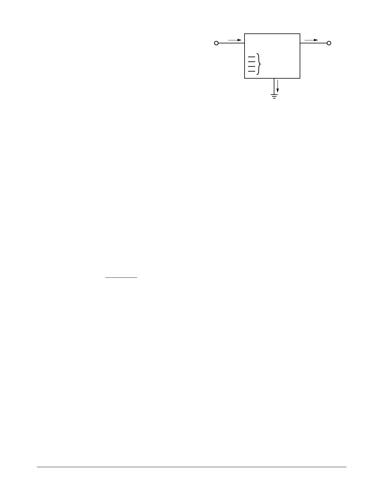
CALCULATING POWER DISSIPATION IN A SINGLE
OUTPUT LINEAR REGULATOR
The maximum power dissipation for a single output
regulator (Figure 14) is:
PD(max) + NJVIN(max) * VOUT(min)NjIOUT(max) ) VIN(max)IQ (1)
where:
VIN(max) is the maximum input voltage,
VOUT(min) is the minimum output voltage,
IOUT(max) is the maximum output current for the
application, and
IQ is the quiescent current the regulator consumes at
IOUT(max).
Once the value of PD(max) is known, the maximum
permissible value of RqJA can be calculated:
RqJA
+
150C *
PD
TA
(2)
The value of RqJA can then be compared with those in the
package section of the data sheet. Those packages with
RqJA’s less than the calculated value in equation 2 will keep
the die temperature below 150°C.
In some cases, none of the packages will be sufficient to
dissipate the heat generated by the IC, and an external
heatsink will be required.
IIN
VIN
IOUT
SMART
REGULATOR®
Control
Features
IQ
VOUT
Figure 14. Single Output Regulator With Key
Performance Parameters Labeled
HEAT SINKS
A heat sink effectively increases the surface area of the
package to improve the flow of heat away from the IC and
into the surrounding air.
Each material in the heat flow path between the IC and the
outside environment will have a thermal resistance. Like
series electrical resistances, these resistances are summed to
determine the value of RqJA.
RqJA + RqJC ) RqCS ) RqSA
(3)
where:
RqJC = the junction−to−case thermal resistance,
RqCS = the case−to−heatsink thermal resistance, and
RqSA = the heatsink−to−ambient thermal resistance.
RqJC appears in the package section of the data sheet. Like
RqJA, it too is a function of package type. RqCS and RqSA are
functions of the package type, heatsink and the interface
between them. These values appear in heat sink data sheets
of heat sink manufacturers.
http://onsemi.com
7
Share Link: