HFA3860B Просмотр технического описания (PDF) - Intersil
Номер в каталоге
Компоненты Описание
Список матч
HFA3860B Datasheet PDF : 40 Pages
| |||
HFA3860B
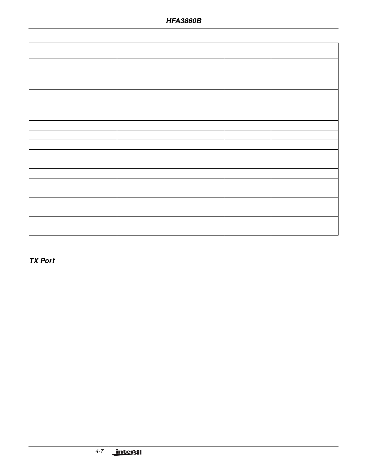
TABLE 1. CONFIGURATION AND CONTROL INTERNAL REGISTER LIST (Continued)
CONFIGURATION
REGISTER
NAME
TYPE
REGISTER
ADDRESS HEX
CR16 (Note 3)
Signal Field (BPSK - 11 Chip Sequence)
R/W
40
or (Cover Code (Low))
CR17 (Note 3)
Signal Field (QPSK - 11 Chip Sequence)
R/W
44
or (Cover Code (High))
CR18
Signal Field (BPSK - Mod. Walsh Sequence)
R/W
48
or (CCK 5.5Mbps)
CR19
Signal Field (QPSK - Mod. Walsh Sequence)
R/W
4C
or (CCK 11Mbps)
CR20
TX Signal Field
R/W
50
CR21
TX Service Field
R/W
54
CR22
TX Length Field (High)
R/W
58
CR23
TX Length Field (Low)
R/W
5C
CR24
RX Status
R
60
CR25
RX Service Field Status
R
64
CR26
RX Length Field Status (High)
R
68
CR27
RX Length Field Status (Low)
R
6C
CR28
Test Bus Address
R/W
70
CR29
Test Bus Monitor
R
74
CR30
Test Register 1, Must Load 00H
R/W
78
CR31
RX Control
R/W
7C
NOTE:
3. To provide CCK functionality, these registers must be programmed in two passes. Once with CR5 bit 7 as a 0 and once with it as a 1.
TX Port
The transmit data port accepts the data that needs to be
transmitted serially from an external data source. The data is
modulated and transmitted as soon as it is received from the
external data source. The serial data is input to the HFA3860B
through TXD using the next rising edge of TXCLK to clock it in
the HFA3860B. TXCLK is an output from the HFA3860B. A
timing scenario of the transmit signal handshakes and
sequence is shown on timing diagram Figure 4.
The external processor initiates the transmit sequence by
asserting TX_PE. TX_PE envelopes the transmit data packet
on TXD. The HFA3860B responds by generating a Preamble
and Header. Before the last bit of the Header is sent, the
HFA3860B begins generating TXCLK to input the serial data
on TXD. TXCLK will run until TX_PE goes back to its inactive
state indicating the end of the data packet. The user needs to
hold TX_PE high for as many clocks as there bits to transmit.
For the higher data rates, this will be in multiples of the
number of bits per symbol. The HFA3860B will continue to
output modulated signal for 2µs after the last data bit is
output, to supply bits to flush the modulation path. TX_PE
must be held until the last data bit is output from the
MAC/FIFO. The minimum TX_PE inactive pulse required to
restart the preamble and header generation is 2.22µs and to
reset the modulator is 4.22µs.
The HFA3860B internally generates the preamble and header
information from information supplied via the control registers.
The external source needs to provide only the data portion of
the packet and set the control registers. The timing diagram of
this process is illustrated on Figure 4. Assertion of TX_PE will
initialize the generation of the preamble and header. TX_RDY,
which is an output from the HFA3860B, is used to indicate to
the external processor that the preamble has been generated
and the device is ready to receive the data packet (MPDU) to
be transmitted from the external processor. Signals TX_RDY,
TX_PE and TXCLK can be set individually, by programming
Configuration Register (CR) 1, as either active high or active
low signals.
The transmit port is completely independent from the
operation of the other interface ports including the RX port,
therefore supporting a full duplex mode.
4-7
Share Link: 