HFA3860A Просмотр технического описания (PDF) - Intersil
Номер в каталоге
Компоненты Описание
Список матч
HFA3860A Datasheet PDF : 39 Pages
| |||
HFA3860A
External Interfaces
There are three primary digital interface ports for the
HFA3860A that are used for configuration and during normal
operation of the device as shown in Figure 1. These ports are:
• The Control Port, which is used to configure, write and/or
read the status of the internal HFA3860A registers.
• The TX Port, which is used to accept the data that
needs to be transmitted from the network processor.
• The RX Port, which is used to output the received
demodulated data to the network processor.
ANTSEL
ANALOG
INPUTS
A/D
REFERENCE
POWER
DOWN
SIGNALS
TEST 8
PORT
HFA3860A
I
I (ANALOG)
Q
Q (ANALOG)
TXD
RSSI (ANALOG) TXCLK
TX_RDY
VREFN
VREFP
RXD
RXC
TX_PE
RX_PE
MD_RDY
CS
SD
RESET
SCLK
R/W
TEST
SDI
TRANSMIT
OUTPUTS
TX_PORT
RX_PORT
CONTROL_PORT
FIGURE 1. EXTERNAL INTERFACE
In addition to these primary digital interfaces the device
includes a byte wide parallel Test Port which can be configured
to output various internal signals and/or data. The device can
also be set into various power consumption modes by external
control. The HFA3860A contains three Analog to Digital (A/D)
converters. The analog interfaces to the HFA3860A include the
In phase (I) and quadrature (Q) data component inputs, and the
RF signal strength indicator input. A reference voltage divider is
also required external to the device.
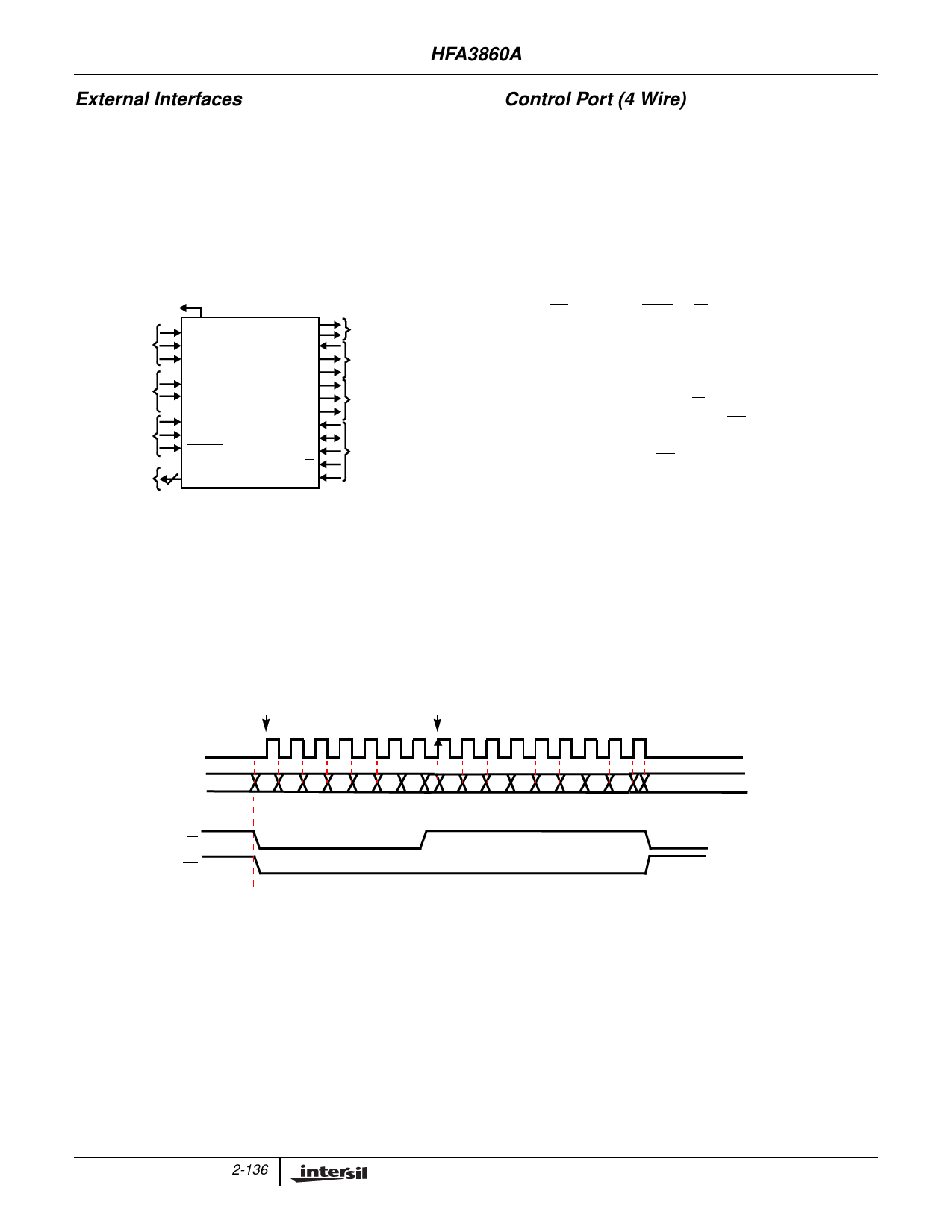
Control Port (4 Wire)
The serial control port is used to serially write and read data
to/from the device. This serial port can operate up to a 11MHz
rate or 1/2 the maximum master clock rate of the device, MCLK
(whichever is lower). MCLK must be running during
programming. This port is used to program and to read all
internal registers. The first 8 bits always represent the address
followed immediately by the 8 data bits for that register. The two
LSBs of address are don’t care, but reserved for future
expansion. The serial transfers are accomplished through the
serial data pin (SD). SD is a bidirectional serial data bus. Chip
Select (CS), and Read/Write (R/W) are also required as
handshake signals for this port. The clock used in conjunction
with the address and data on SD is SCLK. This clock is
provided by the external source and it is an input to the
HFA3860A. The timing relationships of these signals are
illustrated in Figures 2 and 3. R/W is high when data is to be
read, and low when it is to be written. CS is an asynchronous
reset to the state machine. CS must be active (low) during the
entire data transfer cycle. CS selects the serial control port
device only. The serial control port operates asynchronously
from the TX and RX ports and it can accomplish data transfers
independent of the activity at the other digital or analog ports.
The HFA3860A has 31 internal registers that can be configured
through the control port. These registers are listed in the
Configuration and Control Internal Register table. Table 1 lists
the configuration register number, a brief name describing the
register, and the HEX address to access each of the registers.
The type indicates whether the corresponding register is Read
only (R) or Read/Write (R/W). Some registers are two bytes
wide as indicated on the table (high and low bytes).
SCLK
FIRST ADDRESS BIT
FIRST DATABIT OUT
7 6 5 4 3 2 1 07 6 5 4 3 2 1 0
SD
76 54 3 21
7654321 0
MSB
ADDRESS IN
MSB
DATA OUT
LSB
R/W
CS
NOTES:
1. The HFA3860A always uses the rising edge of SCLK. SD, R/W and CS hold times allow the controller to use either the rising or falling edge.
2. This port operates essentially the same as the HFA3824 with the exception that the AS signal of the 3824 is not required.
FIGURE 2. CONTROL PORT READ TIMING
2-136
Share Link: 