HFA3860A Просмотр технического описания (PDF) - Intersil
Номер в каталоге
Компоненты Описание
Список матч
HFA3860A Datasheet PDF : 39 Pages
| |||
HFA3860A
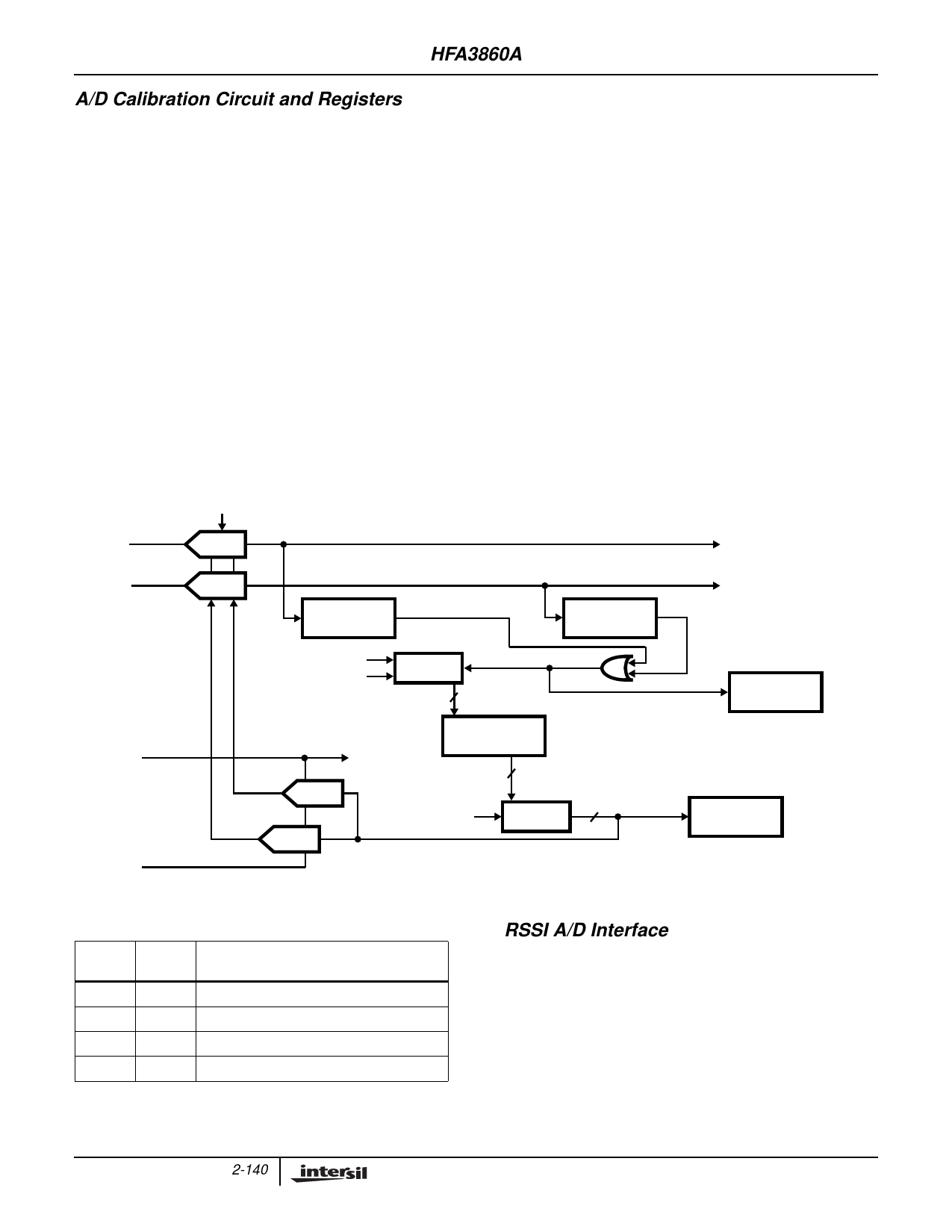
A/D Calibration Circuit and Registers
The A/D compensation or calibration circuit is designed to
optimize A/D performance for the I and Q inputs by
maintaining the full 3-bit resolution of the outputs. There are
two registers (CR 3 AD_CAL_POS and CR 4
AD_CAL_NEG) that set the parameters for the internal I and
Q A/D calibration circuit.
Both I and Q A/D outputs are monitored by the A/D
calibration circuit as shown in Figure 7 and if either has a full
scale value, a 24-bit accumulator is incremented as defined
by parameter AD_CAL_POS. If neither has a full scale
value, the accumulator is decremented as defined by
parameter AD_CAL_NEG. The output of this accumulator is
used to drive D/A converters that adjust the A/D’s
references. Loop gain reduction is accomplished by using
only the 5 MSBs out of the 24 bits. The compensation
adjustment is updated at a 1kHz rate. The A/D calibration
circuit is only intended to remove slow component variations.
For best performance, the optimum probability that either the
I or Q A/D converter is at the saturation level was determined
to be 50%. The probability P is set by the formula:
RX_I_IN
A/D_CK
A/D /
3
RX_Q_IN
A/D
/
3
+FS OR -FS
COMPARE
P(AD_CAL_POS)+(1-P)(AD_CAL_NEG) = 0.
One solution to this formula for P = 1/2 is:
AD_CAL_POS = 1
AD_CAL_NEG = -1
This also sets the levels so that operation with either NOISE
or SIGNAL is approximately the same. It is assumed that the
RF and IF sections of the receiver have enough gain to
cause limiting on thermal noise. This will keep the levels at
the A/D approximately the same regardless of whether
signal is present or not. The A/D calibration is normally set to
work only while the receiver is tracking, but it can be set to
operate all the time the receiver is on or it can be turned off
and held at mid scale.
The A/D calibration circuit operation can be defined through
CR 2, bits 3 and 4. Table 3 illustrates the possible
configurations. The A/D Cal function should initially be
programmed for mid scale operation to preset it, then
programmed for either tracking mode. This initializes the part
for most rapid settling on the appropriate values.
+FS OR -FS
COMPARE
TO CORRELATOR
VREFN
ANALOG
BIASES
VREFP
A/D_CAL_POS
/
8
A/D_CAL_NEG / 8
SELECT
8
TO RSSI A/D
ACCUMULATOR
(25-BIT)
D/A
D/A
A/D_CAL_CK
(APPROX 1KHz)
5 MSBs
REG
5
FIGURE 7. A/D CAL CIRCUIT
TEST REG
MODE 1 (7)
A/DCAL
A/D_CAL_ACCUM
(1/4dB PER LSB)
TEST REG
MODE 25 (8:0)
CR 2
BIT 4
0
0
1
1
TABLE 3. A/D CALIBRATION
CR 2
BIT 3
A/D CALIBRATION CIRCUIT
CONFIGURATION
0 OFF, Reference set at mid scale.
1 OFF, Reference set at mid scale.
0 A/D_Cal while tracking only.
1 A/D_Cal while RX_PE active.
RSSI A/D Interface
The Receive Signal Strength Indication (RSSI) analog signal
is input to a 6-bit A/D, indicating 64 discrete levels of received
signal strength. This A/D measures a DC voltage, so its input
must be DC coupled. Pin 16 (VREFP) sets the reference for
the RSSI A/D converter. VREFP is common for the I and Q
and RSSI A/Ds. The RSSI signal is used as an input to the
Clear Channel Assessment (CCA) algorithm of the
HFA3860A. The RSSI A/D output is stored in an 6-bit register
available via the TEST Bus and the TEST Bus monitor
register. CCA is further described on page 14.
2-140
Share Link: 