CXD2467Q Просмотр технического описания (PDF) - Sony Semiconductor
Номер в каталоге
Компоненты Описание
Список матч
CXD2467Q Datasheet PDF : 38 Pages
| |||
CXD2467Q
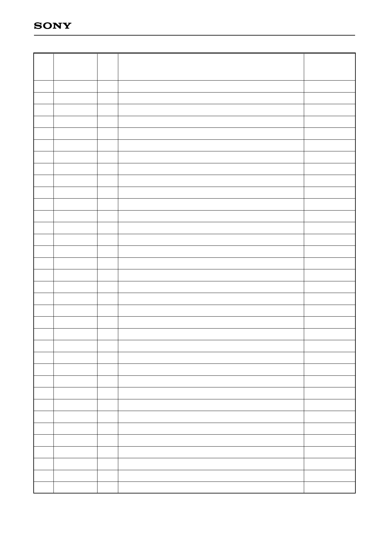
Pin
No.
Symbol
171 PSAVE2
172 R1IN7
173 R1IN6
174 VDD
175 VSS
176 R1IN5
177 R1IN4
178 R1IN3
179 R1IN2
180 R1IN1
181 R1IN0
182 R2IN7
183 R2IN6
184 R2IN5
185 R2IN4
186 VDD
187 VSS
188 R2IN3
189 R2IN2
190 R2IN1
191 R2IN0
192 G1IN7
193 G1IN6
194 G1IN5
195 G1IN4
196 G1IN3
197 G1IN2
198 VSS
199 G1IN1
200 G1IN0
201 G2IN7
202 G2IN6
203 G2IN5
204 G2IN4
205 G2IN3
I/O
Description
I Power saving pin (High: standby status, Low: normal status)
I Red data input (port 1)
I Red data input (port 1)
— Power supply
— GND
I Red data input (port 1)
I Red data input (port 1)
I Red data input (port 1)
I Red data input (port 1)
I Red data input (port 1)
I Red data input (port 1)
I Red data input (port 2)
I Red data input (port 2)
I Red data input (port 2)
I Red data input (port 2)
— Power supply
— GND
I Red data input (port 2)
I Red data input (port 2)
I Red data input (port 2)
I Red data input (port 2)
I Green data input (port 1)
I Green data input (port 1)
I Green data input (port 1)
I Green data input (port 1)
I Green data input (port 1)
I Green data input (port 1)
— GND
I Green data input (port 1)
I Green data input (port 1)
I Green data input (port 2)
I Green data input (port 2)
I Green data input (port 2)
I Green data input (port 2)
I Green data input (port 2)
–9–
Input pin
processing
for open status
L
—
—
—
—
—
—
—
—
—
—
—
—
—
—
—
—
—
—
—
—
—
—
—
—
—
—
—
—
—
—
—
—
—
—
Share Link: 