W742E816 Просмотр технического описания (PDF) - Winbond
Номер в каталоге
Компоненты Описание
Список матч
W742E816 Datasheet PDF : 58 Pages
| |||
W742E/C816
Deleted: SA5505
Deleted: W742C811
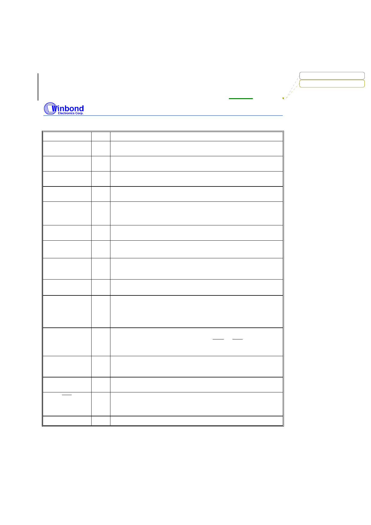
4. PIN DESCRIPTION
SYMBOL
I/O
FUNCTION
XIN2
I Input pin for sub-oscillator.
Connected to 32.768 KHz crystal only.
XOUT2
O Output pin for sub-oscillator with internal oscillation capacitor.
Connected to 32.768 KHz crystal only.
XIN1
I Input pin for main-oscillator.
Connected to 3.58 MHz crystal or resistor to generate system clock.
XOUT1
O Output pin for main-oscillator.
Connected to 3.58 MHz crystal or resistor to generate system clock.
RA0 − RA3
Data_IO
I/O Input/Output port.
Input/output mode specified by port mode 1 register (PM1).
RA.3: Serial data input/output for EEPROM type
RB0 − RB3
I/O Input/Output port.
Input/output mode specified by port mode 2 register (PM2).
RC0 − RC3
I Input port only.
Each pin has an independent interrupt capability.
RD0 − RD3
I Input port only.
This port can release hold mode but can not occur interrupt service
routine.
RE0 − RE3
RF0 − RF3
O Output port only. CMOS type with high sink current capacity for the
LED application.
P00 − P03
I/O Input/Output port.
Input/output mode specified by port mode 6 register (PM6).
P0.0 and P0.1 can be a serial I/O interface selected by SIR register.
P0.0 indicates serial clock, P0.1indicates serial data.
P10 − P13
I Input port only.
Mode
P1.2 & P1.3 indicates hardware interrupt ( INT0 & INT1 )
P1.3: Mode select for EEPROM type
MFP
Output pin only, default in low state.
O This pin can output modulating or nonmodulating frequency, or Timer 1
clock output specified by mode register 1 (MR1).
DTMF/FSK
O This pin can output dual-tone multi-frequency signal for dialing or FSK
signal.
RES
I System reset pin with internal pull-high resistor.
VPP
VPP: supply programming voltage, without internal pull-high resistor for
EEPROM type for avoiding high voltage programming damage
SEG0 − SEG31 O LCD segment output pins.
-6-
Share Link: 