W40S01 Просмотр технического описания (PDF) - Cypress Semiconductor
Номер в каталоге
Компоненты Описание
Список матч
W40S01 Datasheet PDF : 10 Pages
| |||
W40S01-04
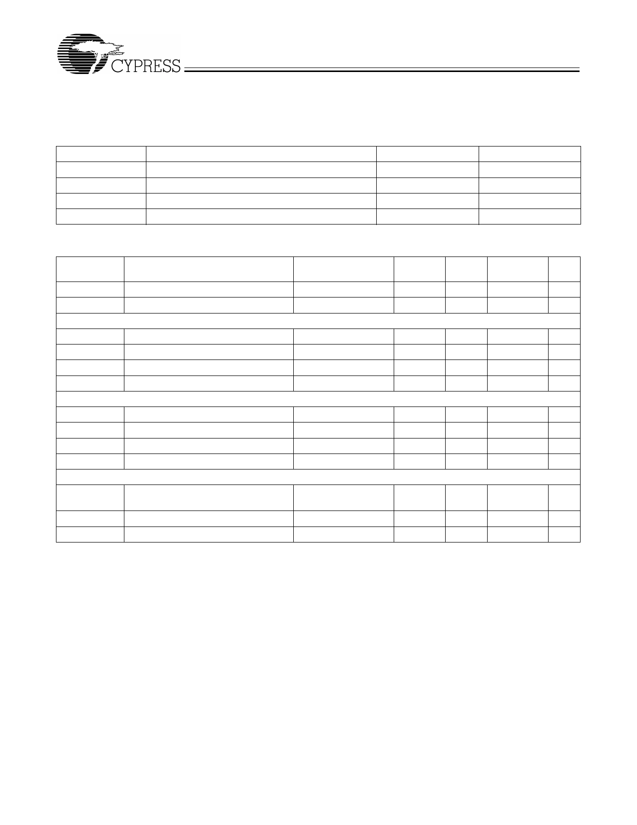
Absolute Maximum Ratings
Stresses greater than those listed in this table may cause per-
manent damage to the device. These represent a stress rating
only. Operation of the device at these or any other conditions
above those specified in the operating sections of this specifi-
cation is not implied. Maximum conditions for extended peri-
ods may affect reliability
Parameter
VDD, VIN
TSTG
TA
TB
Description
Voltage on any pin with respect to GND
Storage Temperature
Operating Temperature
Ambient Temperature under Bias
Rating
Unit
–0.5 to +7.0
V
–65 to +150
°C
0 to +70
°C
–55 to +125
°C
DC Electrical Characteristics: TA = 0°C to +70°C, VDDQ3 = 3.3V±5%
Parameter
Description
Test Condition/
Comments
Min
Typ
Max
Unit
IDD
3.3V Supply Current
BUF_IN = 100 MHz
320
mA
IDD Tristate
3.3V Supply Current in Three-state
BUF_IN = 100 MHz
5
mA
Logic Inputs (BUF_IN, OE, SCLOCK, SDATA)
VIL
Input Low Voltage
VIH
Input High Voltage
IILEAK
Input Leakage Current, BUF_IN
IILEAK
Input Leakage Current[3]
Logic Outputs (SDRAM0:17)[4]
GND–0.3
2.0
–5
–20
0.8
V
VDDQ3+0.5 V
+5
µA
+5
µA
VOL
Output Low Voltage
VOH
Output High Voltage
IOL
Output Low Current
IOH
Output High Current
Pin Capacitance/Inductance
IOL = 1 mA
IOH = –1 mA
VOL = 1.5V
VOH = 1.5V
3.1
70
110
65
100
50
mV
V
185
mA
160
mA
CIN
Input Pin Capacitance (Except
BUF_IN)
5
pF
COUT
Output Pin Capacitance
LIN
Input Pin Inductance
Notes:
3. OE, SCLOCK, and SDATA logic pins have a 250-kΩ internal pull-up resistor (not CMOS level).
4. Outputs loaded by 6" 60Ω transmission lines with 20-pF capacitors.
6
pF
7
nH
8
Share Link: 