IDT723614L30PQF Просмотр технического описания (PDF) - Integrated Device Technology
Номер в каталоге
Компоненты Описание
Список матч
IDT723614L30PQF
Integrated Device Technology

IDT723614L30PQF Datasheet PDF : 39 Pages
| |||
IDT723614 CMOS SyncBiFIFO™ WITH BUS MATCHING AND BYTE SWAPPING
64 x 36 x 2
COMMERCIAL TEMPERATURE RANGE
clock that reads data from the FIFO have not elapsed since the
time the word was written. The empty flag of the FIFO is set
HIGH by the second LOW-to-HIGH transition of the synchro-
nizing clock, and the new data word can be read to the FIFO
output register in the following cycle.
A LOW-to-HIGH transition on an empty flag synchroniz-
ing clock begins the first synchronization cycle of a write if the
clock transition occurs at time tSKEW1 or greater after the write.
Otherwise, the subsequent clock cycle can be the first syn-
chronization cycle (see Figure 13 and 14).
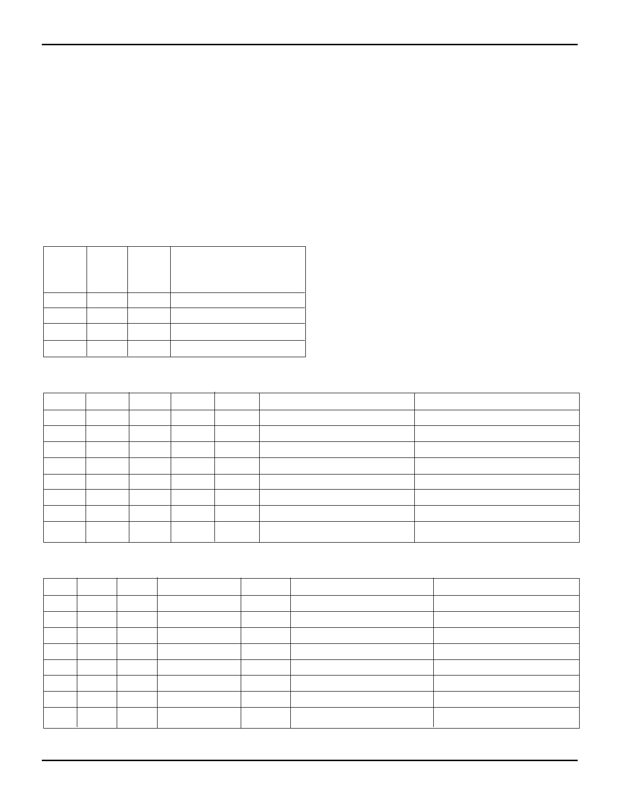
TABLE 1: FLAG PROGRAMMING
ALMOST-FULL AND
FS1 FS0 RST ALMOST-EMPTY FLAG
OFFSET REGISTER (X)
H
H
↑
16
H
L
↑
12
L
H
↑
8
L
L
↑
4
FULL FLAG (FFA, FFB)
The full flag of a FIFO is synchronized to the port clock
that writes data to its array. When the full flag is HIGH, a
memory location is free in the SRAM to receive new data. No
memory locations are free when the full flag is LOW and
attempted writes to the FIFO are ignored.
Each time a word is written to a FIFO, the write pointer is
incremented. The state machine that controls a full flag
monitors a write-pointer and read-pointer comparator that
indicates when the FIFO SRAM status is full, full-1, or full-2.
From the time a word is read from a FIFO, the previous
memory location is ready to be written in a minimum of three
cycles of the full flag synchronizing clock. Therefore, a full flag
is LOW if less than two cycles of the full flag synchronizing
clock have elapsed since the next memory write location has
been read. The second LOW-to-HIGH transition on the full
flag synchronization clock after the read sets the full flag
HIGH and the data can be written in the following clock cycle.
A LOW-to-HIGH transition on a full flag synchronizing
clock begins the first synchronization cycle of a read if the
clock transition occurs at time tSKEW1 or greater after the read.
Otherwise, the subsequent clock cycle can be the first syn-
chronization cycle (see Figure 15 and 16).
TABLE 2: PORT-A ENABLE FUNCTION TABLE
CSA W/RA ENA MBA CLKA
A0-A35 Outputs
H
X
X
X
X
In High-Impedance State
L
H
L
X
X
In High-Impedance State
L
H
H
L
↑
In High-Impedance State
L
H
H
H
↑
In High-Impedance State
L
L
L
L
X
Active, FIFO2 Output Register
L
L
H
L
↑
Active, FIFO2 Output Register
L
L
L
H
X
Active, Mail2 Register
L
L
H
H
↑
Active, Mail2 Register
Port Functions
None
None
FIFO1 Write
Mail1 Write
None
FIFO2 Read
None
Mail2 Read (Set MBF2 HIGH)
TABLE 3: PORT-B ENABLE FUNCTION TABLE
CSB W/RB ENB
SIZ1, SIZ0
CLKB
H
X
X
X
X
L
H
L
X
X
L
H
H
One, both LOW
↑
L
H
H
Both HIGH
↑
L
L
L
One, both LOW
X
L
L
H
One, both LOW
↑
L
L
L
Both HIGH
X
L
L
H
Both HIGH
↑
B0-B35 Outputs
In High-Impedance State
In High-Impedance State
In High-Impedance State
In High-Impedance State
Active, FIFO1 Output Register
Active, FIFO1 Output Register
Active, Mail1 Register
Active, Mail1 Register
Port Functions
None
None
FIFO2 Write
Mail2 Write
None
FIFO1 read
None
Mail1 Read (Set MBF1 HIGH)
7
Share Link: