IDT71028S17Y Просмотр технического описания (PDF) - Integrated Device Technology
Номер в каталоге
Компоненты Описание
Список матч
IDT71028S17Y Datasheet PDF : 7 Pages
| |||
IDT71028
CMOS STATIC RAM 1 MEG (256K x 4-BIT)
COMMERCIAL TEMPERATURE RANGE
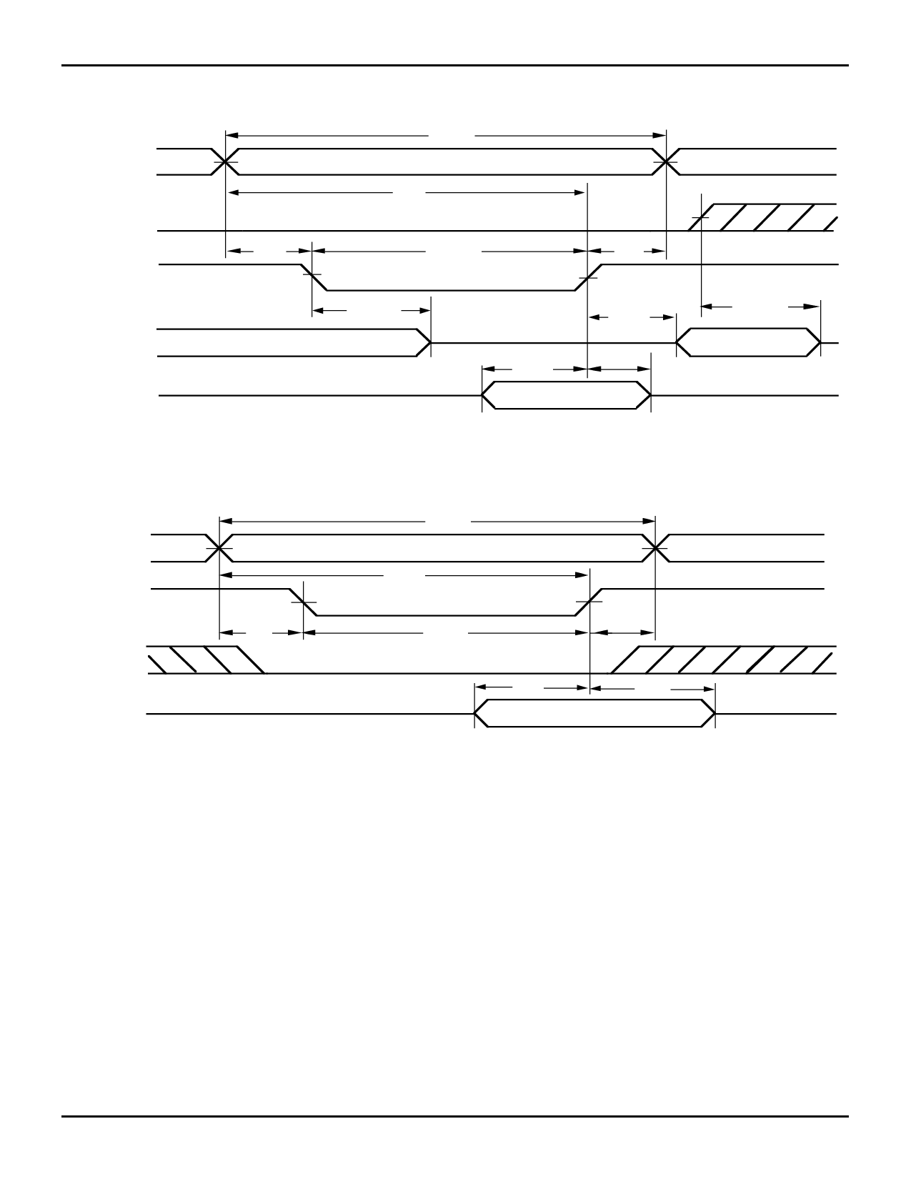
TIMING WAVEFORM OF WRITE CYCLE NO.1 (WE CONTROLLED TIMING)(1,2,3,5)
ADDRESS
CS
WE
DATAOUT
DATAIN
tWC
tAW
tAS
tWP(3)
tWR
tWHZ (6)
tOW (6)
(4)
HIGH IMPEDANCE
tDW
tDH
DATAIN VALID
tCHZ (6)
(4)
2966 drw 07
TIMING WAVEFORM OF WRITE CYCLE NO.2 (CS CONTROLLED TIMING)(1,2,5)
tWC
ADDRESS
tAW
CS
tAS
tCW
tWR
WE
DATAIN
tDW
tDH
DATAIN VALID
2966 drw 08
NOTES:
1. WE or CS must be HIGH during all address transitions.
2. A write occurs during the overlap of a LOW CS and a LOW WE.
3. OE is continuously HIGH. If during a WE controlled write cycle OE is LOW, tWP must be greater than or equal to tWHZ + tDW to allow the I/O drivers to turn
off and data to be placed on the bus for the required tDW. If OE is HIGH during a WE controlled write cycle, this requirement does not apply and the
minimum write pulse is as short as the specified tWP.
4. During this period, I/O pins are in the output state, and input signals must not be applied.
5. If the CS LOW transition occurs simultaneously with or after the WE LOW transition, the outputs remain in a high-impedance state.
6. Transition is measured ±200mV from steady state.
9.4
6
Share Link: 