IDT72141L35P Просмотр технического описания (PDF) - Integrated Device Technology
Номер в каталоге
Компоненты Описание
Список матч
IDT72141L35P Datasheet PDF : 13 Pages
| |||
IDT72131, IDT72141
CMOS PARALLEL-TO-SERIAL FIFO 2048 x 9 & 4096 x 9
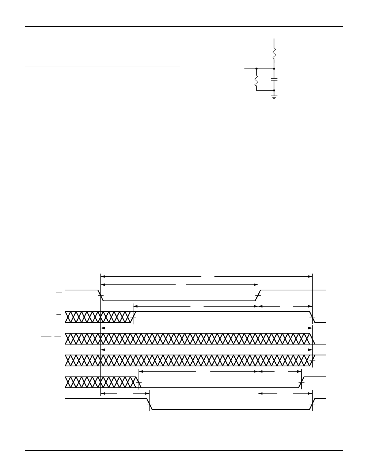
AC TEST CONDITIONS
Input Pulse Levels
Input Rise/Fall Times
Input Timing Reference Levels
Output Reference Levels
Output Load
GND to 3.0V
5ns
1.5V
1.5V
See Figure A
2751 tbl 08
COMMERCIAL TEMPERATURE RANGES
5V
D.U.T.
680Ω
1.1KΩ
30pF*
2751 drw 03
or equivalent circuit
Figure A. Ouput Load
*Including jig and scope capacitances
FUNCTIONAL DESCRIPTION
Parallel Data Input
The data is written into the FIFO in parallel through the
D0-8 input data lines. A write cycle is initiated on the falling
edge of the Write (W) signal provided the Full Flag (FF) is not
asserted. If the W signal changes from HIGH-to-LOW and the
Full-Flag (FF) is already set, the write line is inhibited internally
from incrementing the write pointer and no write operation
occurs.
Data set-up and hold times must be met with respect to the
rising edge of Write. The data is written to the RAM at the write
pointer. On the rising edge of W, the write pointer is
incremented. Write operations can occur simultaneously or
asynchronously with read operations.
Serial Data Output
The serial data is output on the SO pin. The data is clocked
out on the rising edge of SOCP providing the Empty Flag (EF)
is not asserted. If the Empty Flag is asserted then the next data
word is inhibited from moving to the output register and being
clocked out by SOCP. NOTE: SOCP should not be clocked
once the last bit of the last word has been clocked out. If it is,
then two things will occur. One, the SO pin will go High-Z and
two, SOCP will be out of sync with Next Read (NR).
The serial word is shifted out Least Significant Bit first, that
is the first bit will be D0, then D1 and so on up to the serial word
width. The serial word width must be programmed by connect-
ing the appropriate Data Set line (Q4, Q6, Q7 or Q8) to the NR
input. The Data Set lines are taps off a digital delay line.
Selecting one of these taps, programs the width of the serial
word to be read and shifted out.
RS
W
AEF, EF
HF, FF
SOCP
Q4, Q6, Q7, Q8
tRSQL
tRSC
tRS
tRSS
tRSF1
tRSF2
tRSS
Figure 1. Reset
tRSR
tRSR
tRSQH
2751 drw 04
5.34
5
Share Link: 