CDP1883 Просмотр технического описания (PDF) - Intersil
Номер в каталоге
Компоненты Описание
Список матч
CDP1883 Datasheet PDF : 6 Pages
| |||
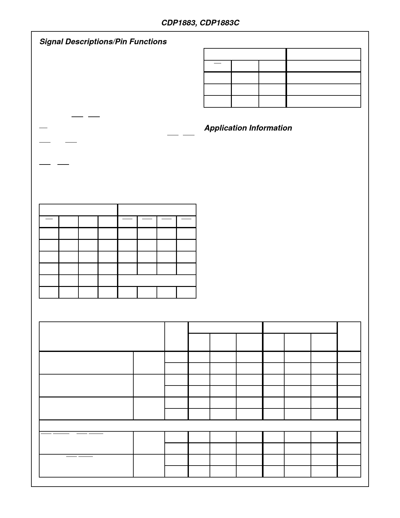
CDP1883, CDP1883C
Signal Descriptions/Pin Functions
TRUTH TABLE
CLOCK: Latch Input Control - a high on the clock input will
allow data to pass through the latch to the output pin. Data is
latched on the high-to-low transition of the clock input. This
pin is connected to TPA in CDP1800-series systems and tied
to VDD for other applications.
MA0 - MA4: Address inputs to the high-byte address
latches.
INPUTS
CE
CLK MA0 - 4
X
1
1
X
1
0
X
0
X
OUTPUTS
A8 - A12
1
0
Previous State
MA5 - MA6: High byte address inputs decoded to produce
chip selects CS0 - CS3.
CE: CHIP ENABLE input - A low on this pin will enable the
chip select decoder. A high on this pin forces CS0, CS1,
CS2, and CS3 outputs to a high (false) state.
A8 - A12: Latched high-byte address outputs.
CS0 - CS3: One of four latched and decoded Chip Select
outputs.
VDD, VSS: Power and ground pins, respectively.
TRUTH TABLE
INPUTS
OUTPUTS
CE CLK MA5 MA6 CS0 CS1 CS2 CS3
0
1
0
0
0
1
1
1
0
1
1
0
1
0
1
1
0
1
0
1
1
1
0
1
0
1
1
1
1
1
1
0
X = Don’t Care
Application Information
The CDP1883 and CDP1883C can be interfaced, without
external components, with CDP1800-series microprocessor
systems. These microprocessors feature a multiplexed
address bus and provide an address latch signal (TPA) that
is used as the clock input of the CDP1883. See Figure 2 and
Figure 3.
This signal is used to latch 7 bits of the high-order address.
The lower five high-order address inputs are latched and
held to be used with the eight lower-order address inputs to
access an 8K x 8-bit memory. The two upper high-order
address inputs are latched and decoded for use as chip
selects.
The latched address and decoding functions of the
CDP1883 and CDP1883C allow them to operate with 32K-
byte memory systems. In addition, smaller memory systems
can be configured with 4K x 8-bit or smaller memories, or a
mix of memory sizes up to 8K x 8-bit.
0
0
X
X
Previous State
1
X
X
X
1
1
1
1
Dynamic Electrical Specifications TA = -40oC to +85oC, VDD ± 5%, tR, tF = 20ns, VIH = 0.7 VDD, VIL = 0.3 VDD, CL = 100pF.
See Figure 1
CDP1883
CDP1883C
PARAMETER
VDD
(NOTE 1) (NOTE 2)
(NOTE 1) (NOTE 2)
(V)
MIN
TYP
MAX
MIN
TYP
MAX UNITS
Minimum Setup Time,
Memory Address to CLOCK
tMACL
5
-
10
35
-
10
35
ns
10
-
8
25
-
-
-
ns
Minimum Hold Time,
Memory Address After CLOCK
tCLMA
5
-
8
25
-
8
25
ns
10
-
8
25
-
-
-
ns
Minimum CLOCK Pulse Width
tCLCL
5
-
50
75
-
50
75
ns
10
-
25
40
-
-
-
ns
PROPAGATION DELAY TIMES
Chip Enable to Chip Select
tCECS
5
-
75
150
-
75
150
ns
10
-
45
100
-
-
-
ns
CLOCK to Chip Select
tCLCS
5
-
100
175
-
100
175
ns
10
-
65
125
-
-
-
ns
4-132
Share Link: 