ISP1563 Просмотр технического описания (PDF) - Infineon Technologies
Номер в каталоге
Компоненты Описание
Список матч
ISP1563 Datasheet PDF : 36 Pages
| |||
TDK5116F
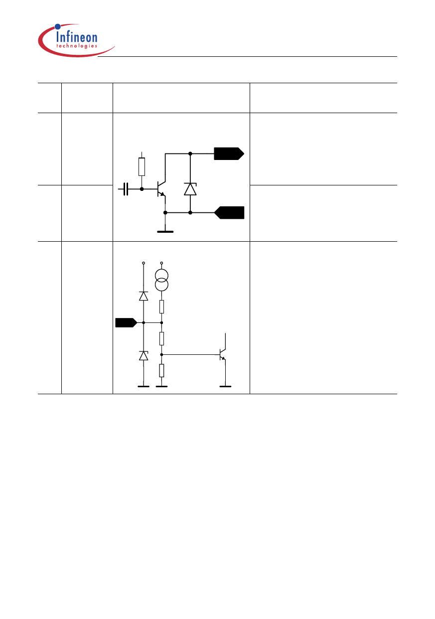
Functional Description
Pin Symbol
No.
8 PAGND
9 PAOUT
10 PDWN
Interface Schematic
Function
Ground connection of the power
amplifier.
9 The RF ground return path of the
power amplifier output PAOUT
(pin 9) has to be concentrated to
this pin.
RF output pin of the transmitter.
8 A DC path to the positive supply
VS has to be supplied by the
antenna matching network.
Disable pin for the complete
VS
transmitter circuit.
40 µA ∗ (ASKDTA+FSKDTA) A logic low (PDWN < 0.7 V) turns
off all transmitter functions.
5 kΩ
10
A logic high (PDWN > 1.5 V) gives
"ON" access to all transmitter functions.
150 kΩ
250 kΩ
PDWN input will be pulled up by
40 µA internally by either setting
FSKDTA or ASKDTA to a logic
high-state.
1) Indicated voltages and currents apply for PLL Enable Mode and Transmit Mode.
In Power Down Mode, the values are zero or high-ohmic.
Data Sheet
11
V 1.1, 2006-09-15
Share Link: 