TB2104F Просмотр технического описания (PDF) - Toshiba
Номер в каталоге
Компоненты Описание
Список матч
TB2104F Datasheet PDF : 9 Pages
| |||
TB2104F
· In T-BUS mode, start data transmission with the LS terminal (period) set at “L” level.
Thereafter, send address data 8 bits, display data 20 bits, and chip select code 4 bits, synchronizing with rise
of CLK signal.
· After sending data, set the LS terminal to “L” level again and terminate the data sending.
· On a driver IC when chip select code agrees with chip select code by AD1 / AD2, display data are updated at
fall of LS signal.
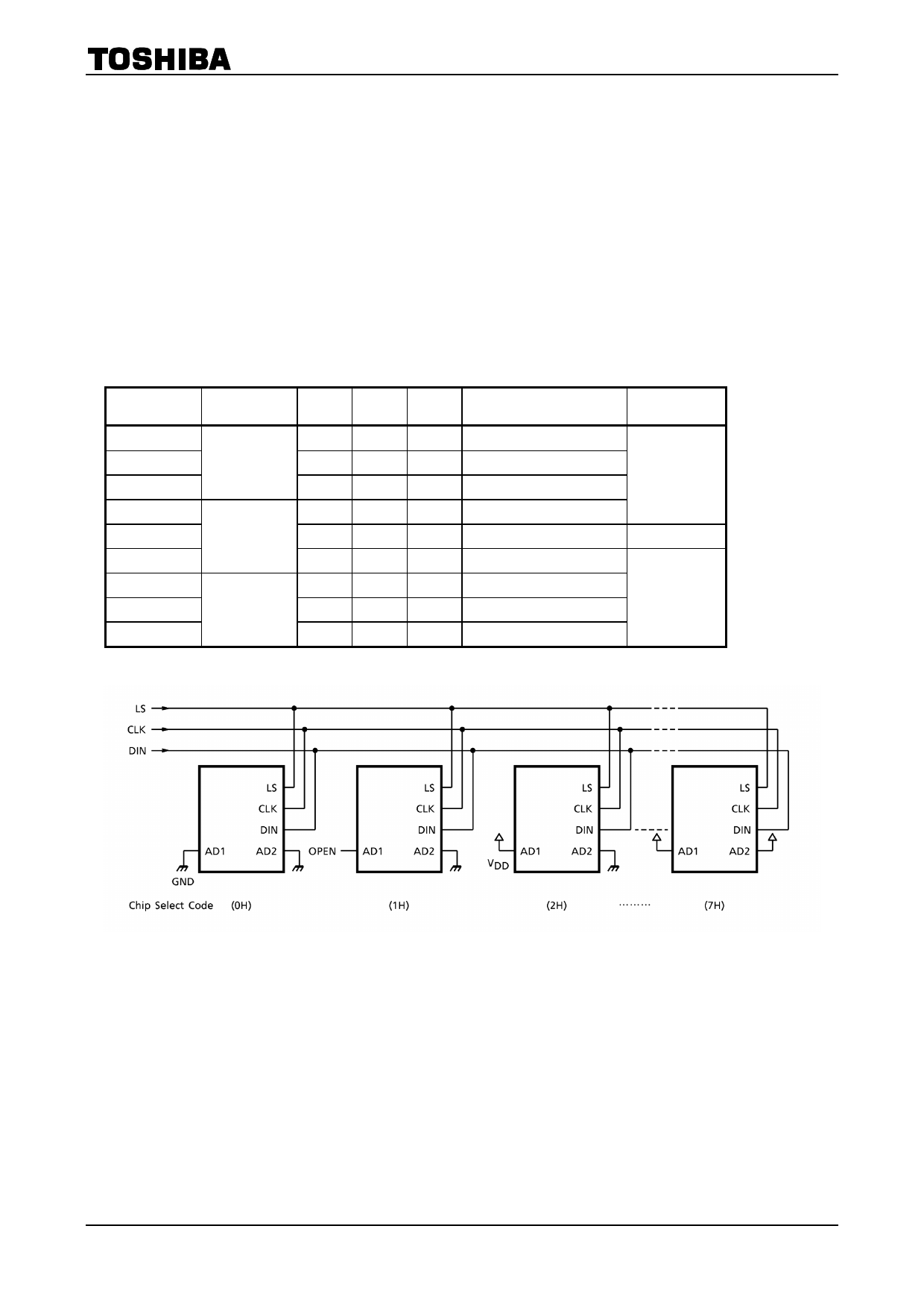
· When increasing driver ICs, it is possible to connect up to 8 ICs on the same bus line in combination with
AD1 / AD2.
· T-BUS address of the TB2104F is “D4H”.
· When data are transferred using T-BUS address “00H”, the data can be input to all the driver ICs on the
bus line independently of chip select codes (“0H”~“7H”). (This function can be used for power on reset.)
3. AD1 / AD2 input and chip select codes
AD1 / AD2 input are 3-value level inputs and 9 kinds (3×3) of codes can be set.
AD1
VIH
VIM
VIL
VIH
VIM
VIL
VIH
VIM
VIL
AD2
A
B
C
Chip Select Code
1
1
1
“7H”
VIH
0
1
1
“6H”
1
0
1
“5H”
0
0
1
“4H”
VIM
—
—
—
—
1
1
0
“3H”
0
1
0
“2H”
VIL
1
0
0
“1H”
0
0
0
“0H”
4. Example of extension of driver ICs in T-BUS mode chip select code
Mode
T-BUS
Serial
T-BUS
4
2002-10-30
Share Link: 