SN74LS161AML1 Просмотр технического описания (PDF) - ON Semiconductor
Номер в каталоге
Компоненты Описание
Список матч
SN74LS161AML1 Datasheet PDF : 6 Pages
| |||
SN54/74LS160A • SN54/74LS161A
SN54/74LS162A • SN54/74LS163A
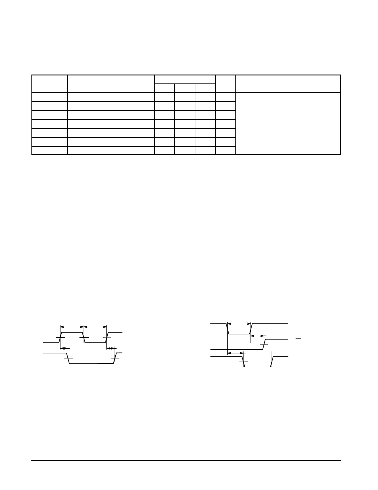
AC SETUP REQUIREMENTS (TA = 25°C)
Symbol
Parameter
tWCP
Clock Pulse Width Low
tW
MR or SR Pulse Width
ts
Setup Time, other*
ts
Setup Time PE or SR
th
Hold Time, data
th
Hold Time, other
trec
Recovery Time MR to CP
*CEP, CET or DATA
Limits
Min Typ Max Unit
25
ns
20
ns
20
ns
25
ns
3
ns
0
ns
15
ns
Test Conditions
VCC = 5.0 V
DEFINITION OF TERMS
SETUP TIME (ts) — is defined as the minimum time required
for the correct logic level to be present at the logic input prior to
the clock transition from LOW to HIGH in order to be recog-
nized and transferred to the outputs.
HOLD TIME (th) — is defined as the minimum time following
the clock transition from LOW to HIGH that the logic level must
be maintained at the input in order to ensure continued recog-
nition. A negative HOLD TIME indicates that the correct logic
level may be released prior to the clock transition from LOW to
HIGH and still be recognized.
RECOVERY TIME (trec) — is defined as the minimum time re-
quired between the end of the reset pulse and the clock transi-
tion from LOW to HIGH in order to recognize and transfer
HIGH Data to the Q outputs.
AC WAVEFORMS
CP
Q
tW(H)
1.3 V
tW(L)
tPHL
1.3 V
1.3 V
tPLH
OTHER CONDITIONS:
PE = MR (SR) = H
CEP = CET = H
1.3 V
Figure 1. Clock to Output Delays, Count
Frequency, and Clock Pulse Width
tW
MR 1.3 V
CP
⋅ ⋅ ⋅ Q0 Q1 Q2 Q3
tPHL
trec
1.3 V
OTHER CONDITIONS:
PE = L
P0 = P1 = P2 = P3 = H
1.3 V
Figure 2. Master Reset to Output Delay, Master Reset
Pulse Width, and Master Reset Recovery Time
FAST AND LS TTL DATA
5-282
Share Link: 