SM5168 Просмотр технического описания (PDF) - Nippon Precision Circuits
Номер в каталоге
Компоненты Описание
Список матч
SM5168 Datasheet PDF : 9 Pages
| |||
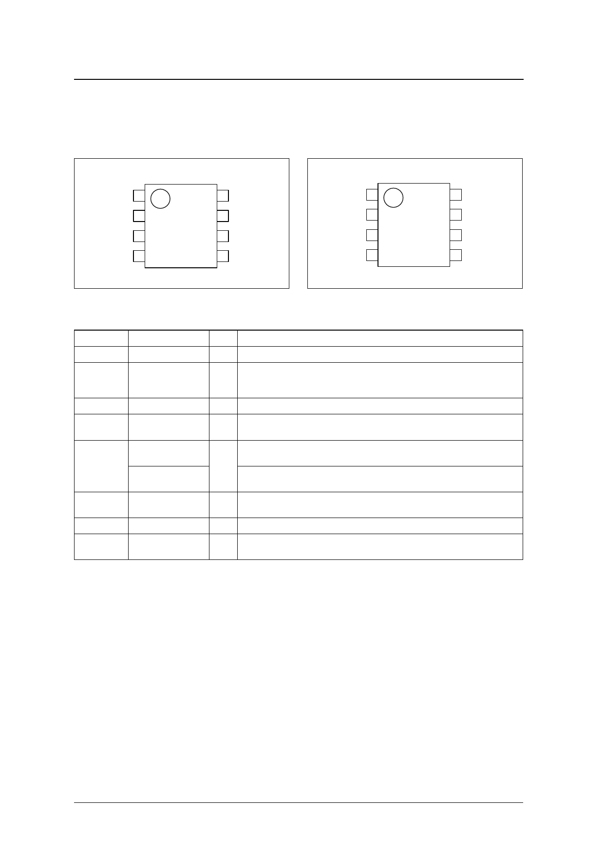
PINOUT
(Top view)
SM5168A× series
SM5168 series
SM5168C× series
VDD 1
DO 2
VSS 3
FIN 4
8 XIN
7 LD
6 TEST
5 OPR
VDD 1
DO 2
VSS 3
FIN 4
8 XIN
7 LD
6 TEST
5 TR
PIN DESCRIPTION
Number
1
2
3
4
5
6
7
8
Name
VDD
DO
VSS
FIN
OPR
(SM5168A× series)
TR
(SM5168C× series)
TEST
LD
XIN
I/O
Description
– 2.7 to 3.6V supply
Phase comparator error signal three-state output pin.
O Built-in charge pump means that this output can be connected to a low-pass filter. The output
polarity is preset for connection to a passive filter.
– Ground pin
I
Phase comparator frequency divider (N-counter) signal input pin.
Feedback resistor built-in, so input can be AC-coupled.
Power-save control pin.
Start when HIGH, standby mode when LOW.
I
Frequency divider switching control.
Switches between 2 sets of reference and comparator frequency dividers.
I
Test pin.
Leave open or connect to VSS for normal operation.
O Unlock signal output pin. (Unlocked when LOW)
I
Reference frequency divider (R-counter) external clock input pin.
Feedback resistor built-in, so input can be AC-coupled.
SEIKO NPC CORPORATION —2
Share Link: 